Abstract
This paper introduces an innovative two-stage distributed RC oscillator design, enhancing the noise performance and frequency stability for compact electronic devices. This work significantly reduces the comparator noise and improves system reliability by implementing a novel approach to increase the signal transition slope, coupled with optimized resistor and capacitor configurations. The study employs a quadrature oscillator topology and a precise reference voltage generation method, effectively addressing the challenges of mismatch and noise performance. A 469.2 kHz quadrature oscillator with two-stage distributed RC is implemented with a 0.18 μm CMOS process, achieving a FoM of −160 dBc/Hz at 100 Hz with a stable −20 dB roll-off in the phase noise and an Allan deviation floor of less than 0.7 ppm.
Keywords: relaxation oscillator; RC network; RC oscillator; low noise; low power; phase noise; frequency-locked loop
1. Introduction
RC oscillators have gained significant popularity as reference frequency generators in compact wearable and implantable devices [1,2]. This widespread use stems from their inherent ability to provide a highly controllable, untrimmed frequency. Their reliability on low-cost circuitry makes them particularly appealing for such applications, making them an economical choice for designers. The concept of a closed-loop architecture of a frequency-lock loop (FLL) has been introduced as an innovative solution to overcome the challenge of nonzero circuit delays and process variation [3,4,5,6,7]. The technical workings of the architecture involve converting the output frequency based on RC values into a corresponding voltage. This voltage is then compared to a reference voltage derived from a carefully designed resistor-based supply divider, generating a voltage error close to zero by the negative feedback characteristics. This approach ensures that the oscillation period remains stable and is predominantly determined by the RC values, a crucial factor in maintaining a consistent performance. Despite the advantages of the feedback mechanism, especially its effectiveness in compensating the effects of the comparator’s thermal noise and circuit delays, the performance ceiling of the system is, in fact, limited by the inherent noise and power characteristics of the analog circuits tasked with managing the feedback voltage error. This is a critical bottleneck that often restricts the overall effectiveness of the system.
Various alternative methods have been proposed to achieve a low-noise oscillator, such as a boosted swing during the RC transient phase [8,9,10], a feedback [3,4,5,7] and a chopping [5] method. The core idea of the boosted swing is to significantly increase the signal slope at the comparator input. This increase is a strategy to reduce the impact of the comparator noise, thereby improving the overall noise performance [11,12,13,14,15]. However, while this method seems promising on paper, its practical implementation is challenging.
Traditional boosting schemes face a significant issue when integrated with feedback loop systems due to the need for extra circuits to extract frequency information from the boosted voltage signal. Using the boosted voltage that exceeds ground or supply voltages results in the forward biasing of parasitic PN junctions of the MOS transistor, an unwanted situation that can trigger various problems. Consequently, due to this technical obstacle, boosting schemes often bypass the feedback loop and opt for a high-speed comparator instead [9]. This comparator plays a vital role in diminishing the impact of circuit delay, a compromise essential for preserving system integrity and performance.
Implementing low-frequency RC oscillators also brings its own set of challenges. When the oscillator’s frequency drops, so does the number of cycles within the 1/f corner frequency period. This reduced oscillator’s frequency deteriorates the thermal noise’s averaging effect and degrades frequency stability. Furthermore, the static power consumed by critical analog circuits and leakage currents does not scale proportionally with the output frequency. As a result, while there are some instances of kHz oscillators with outstanding figures of merit (FoM), the MHz oscillators have shown themselves to be competitive with the best in the field.
This study introduces a distributed RC oscillator designed to make the signal transition slope sharper by mimicking a sinusoidal waveform through second-order band-pass tuning. Since the proposed RC network is very similar to the distributed RC model of the transmission line, this paper describes it as the distributed RC network. The oscillation frequency band receives an additional boost with the inclusion of more RC segments. This newly developed frequency-tuned distributed RC network is then integrated into a quadrature oscillator. The oscillator, fabricated in 0.18 μm CMOS, achieves a FoM of −160 dBc/Hz at 100 Hz with a stable −20 dB roll-off in the phase noise and an Allan deviation floor of less than 0.6 ppm.
This paper consists of six sections. Section 2 demonstrates the concept of the proposed transition slope boosting with a two-stage distributed RC network and its expanded topology. Section 3 describes the circuit implementation of the proposed two-stage distributed RC oscillator. Section 4 summarizes the measurement results, followed by a discussion in Section 5. Finally, the paper concludes with Section 6, which encapsulates the findings and implications of the work.
2. Design Strategies
2.1. Proposed Two-Stage Distributed RC Network
The noise performance of an RC oscillator is predominantly influenced by the signal transition slope at the comparator input [7]. A rapid transition slope at the comparator input can result in a high frequency-to-voltage gain for the feedback loop because it can generate a significant voltage difference from a minimal period change. If so, it can improve the signal-to-noise ratio and enhance the noise performance. Additionally, it can decrease the comparison time for a small input voltage difference that the noise can easily influence in the comparison region. A shorter comparison time can diminish the impact of the thermal noise. Therefore, increasing the transition slope can effectively improve the noise performance. Figure 1 illustrates the motivation for the proposed approach, simulating a sinusoidal transition using a distributed RC network. Unlike a traditional first-order lumped RC line that continuously decreases the slope from the start of the transition, 0 or TOSC/2 time, a sinusoid reaches its maximum transition slope as it crosses the center voltage. If a voltage comparison is conducted at TOSC/2, an appropriate phase shift of the sinusoid can enhance the slope, which is equivalent to the −π. This research utilizes a distributed RC network to mimic a sinusoidal transition and proposes a design strategy to achieve a maximum phase shift close to −π. The concept of the proposed circuit is illustrated using a two-stage distributed RC line comprising two resistors, R1 and R2, and two capacitors, C1 and C2 (Figure 2). It has two signal paths: the first path travels through R1 and R2 with the input signal (Vin) and the second through the C1, followed by R2 with the complementary input signal (−Vin). The first path, named a resistor path (HR), exhibits a second-order low-pass characteristic, whereas the second path, named a capacitor path (HC), demonstrates a band-pass characteristic.
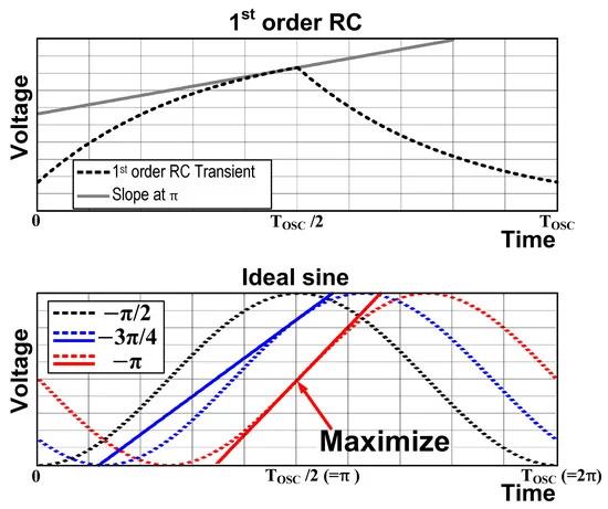
Figure 1. Concept of the proposed transition slope boosting with a phase-shifted sinusoid.
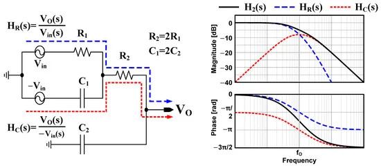
Figure 2. The circuit diagram and the frequency responses of the two-stage distributed RC network.
The transfer functions of the paths are derived as follows:
The ω0 and Q represent the resonance frequency and quality factor of the proposed second-order transfer functions, respectively. The overall transfer function is the sum of HR and HC, which is denoted by H2 in Figure 2. Generally, the Q factor indicates the performance of oscillation. Therefore, maximizing the Q factor is anticipated to enhance the oscillation performance. Determining the appropriate values for the resistors and capacitor values is crucial to achieving a high Q factor. The values for the resistors and capacitors can be defined as follows:
R2=m·R1(6)
C2=n·C1(7)
Consequently, the quality factor can be reformulated as:
Q=11mn√+mn−−−√+nm−−√(8)
Interestingly, the quality factor is determined solely by the ratio of the resistors and capacitors. The denominator value should be minimized to maximize the Q. For a simplified analysis, the denominator can be broken down into 1/mn−−−√+mn−−−√and n/m−−−−√
. Given that m and n are positive, 1/mn−−−√+mn−−−√
is minimized when the mn equals 1. n/m−−−−√
is minimized with a large m and a small n. So, a larger quality factor can be achieved with a larger R2 compared to R1 and a smaller C2 compared to C1.
The transfer curves depicted in Figure 2 are the simulated results obtained with R2 = 2R1 (m = 2) and C2 = C1/2 (n = 1/2), in alignment with the previous analysis. As shown in the transfer curve, the phase response of HR eventually approaches −π as the frequency increases, which is two times larger than the first-order lumped RC, which maximally shifts the phase by −π/2. However, the amount of the phase shift at the resonance frequency, ωO, is insufficient only with HR. The overall phase shift can be further enlarged by HC. The ωO is the passband center of HC, where the phase shift is −π. This analysis reveals a design strategy for R1, R2, C1 and C2. The analysis shows that the optimal condition can be achieved when R1C1 and R2C2 are equal, with R1C2 minimized. With this condition, the overall transfer function H2 exhibits a boosted gain at ωO with a phase shift of −3π/4 which is close to −π.
Figure 3 shows the transient response of the proposed two-stage distributed RC network when step inputs from 0 to VDD and from VDD to 0 are applied to the resistor path (HR) and the capacitor path (HC), respectively. It is assumed that the voltage swing initiates from VDD/3 and ends at 2VDD/3. The proposed RC network shows a sinusoid-like step response, compared with that of the first-order RC network, such that the output voltage decreases initially and then rises, effectively enhancing the slope at the end voltage at the half period (TOSC/2). It shows a 2.28 times improvement in the transition slope at the target voltage level crossing the end voltage.
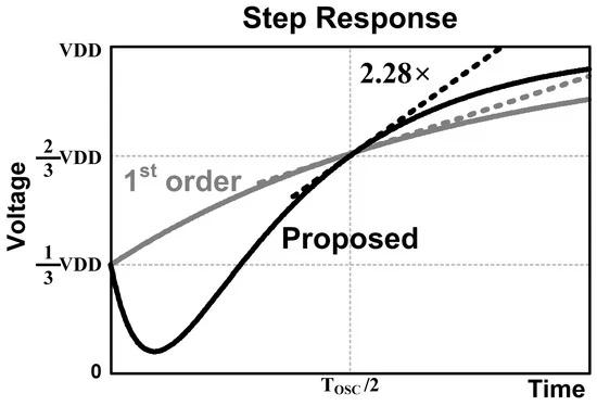
Figure 3. Step response of the conventional first-order and proposed RC network.
2.2. Multiple Stages of the Distributed RC Network
A simulation is performed with an expanded topology of the distributed RC network to verify the effect of the RC design. Figure 4 shows an N-stage distributed RC network. Complementary input voltage signals propagate through the resistor path and capacitor path, representing their transfer functions of HRN and HCN, respectively. The overall transfer function denoted as HN is the sum of HRN and HCN.
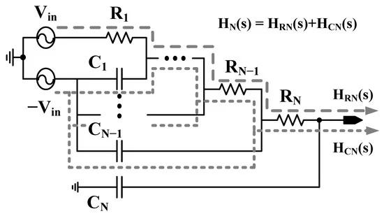
Figure 4. Circuit diagram of the N-stage distributed RC network.
Figure 5 shows the frequency responses of the two-, four- and six-stage distributed RC network (N = 2, 4 and 6). It reveals that the magnitude of the capacitor path frequency response escalates with an increase in the number of stages, consequently boosting the magnitude of the overall transfer function at the oscillation frequency. Figure 6 presents the transient responses triggered by applying the same step input signal with the same initial and end voltages, as shown in Figure 3. It demonstrates that the transient slope at Tosc/2 becomes steeper as the number of stages increases. However, the numerous stages in the distributed RC network tend to push the swing voltage below the ground voltage. If the drain or source of an MOSFET is connected to the swing node for voltage sampling, this is critical because the negative voltage can result in a forward bias for the MOSFET’s parasitic PN junction at the drain or source. Additionally, the multiple stages might cause a significant difference between the smallest and largest capacitors or resistors, leading to an overall larger area requirement.

Figure 5. Frequency responses of the two-, four-, and six-stage distributed RC network.

Figure 6. Step responses of the two-, four- and six-stage distributed RC network.
Figure 7 shows the six-stage distributed RC network. The resistor path’s transfer function is HR, and that of the capacitor paths are HC1, HC2, HC3, HC4 and HC5. The overall transfer function denoted as H6 is the sum of HR and HC. The design strategy determining the values of resistors and capacitors is important. So, Figure 8 summarizes the results with four cases of resistor and capacitor sizing: (i) Rn = 2Rn−1 and Cn = Cn−1/2, (ii) Rn = 2Rn−1 and Cn = 2Cn−1, (iii) Rn = Rn−1/2 and Cn = Cn−1/2 and (iv) Rn = Rn−1/2 and Cn = 2Cn−1. All the transfer functions from each capacitor (HC1~HC5) follow the second-order band-pass characteristics. Case (i) shows that all transfer functions of the capacitor paths have large Q-factors (0.19~0.36) and a high gain, with all the passband centers being well aligned. In case (ii), the transfer functions of the capacitor paths have almost the same center frequency. However, the gain of former stages exponentially decreases, resulting in low Q-factors (0.17~0.19) in the overall transfer function. Case (iii) also shows similar center frequencies, but the passbands are too wide with low Q-factors (0.065~0.077). In case (iv), though the transfer functions have the largest gain with low Q-factors (0.018~0.019), the center frequencies are not tuned. From these results, case (i) achieves both aligned tuning and a large gain. It is well matched with the analysis of the two-stage distributed RC network in Section 2.1. Figure 9 shows the step response of the four cases. It is assumed the initial voltage is VDD/3 and the end voltage is 2·VDD/3. It shows that the design strategy of the resistors and capacitors dramatically influences the transient slope.
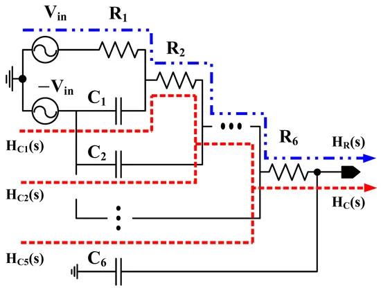
Figure 7. Circuit diagram of the six-stage distributed RC network and the signal path through the resistors and capacitors.

Figure 8. Frequency responses of the generalized topology for four cases with different values of resistors and capacitors of N-stage distributed RC network.
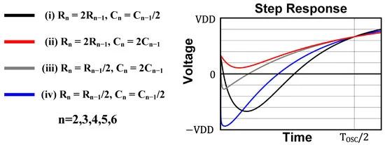
Figure 9. Step responses of the generalized topology of resistors and capacitors value of N-stage distributed RC network.
3. The Proposed Two-Stage Distributed RC Oscillator
Figure 10 illustrates the circuit diagram of the proposed distributed RC oscillator. A quadrature oscillator topology [7] is adopted with the two-stage distributed RC network for a sinusoid emulation. The quadrature oscillator consists of a signal generation block and a reference generation block. In the signal generation block, the quadrature phase is generated with two identical distributed RC networks and four comparators receiving reference voltages, VLU1, VLD1, VLU2 and VLD2, provided by the reference generation block (details in Section 3.1). The outputs of the distributed RC network, VO1 and VO2, are sampled when the output status of the comparators changes and are compared with the target swing defined by VUP and VDN. The Gm amplifiers process errors and update the reference voltages, VLU1, VLD1, VLU2 and VLD2. This feedback architecture adaptively controls the reference voltages to set VO1 and VO2 as VUP or VDN at the sampled transition, providing a stable oscillation period.
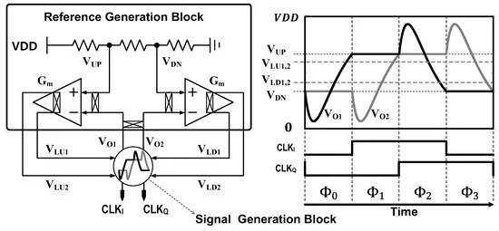
Figure 10. The overall architecture and the waveform of the proposed distributed RC oscillator.
3.1. Quadrature Signal Generation
The signal generation block has two identical sub-oscillators that alternately swing the voltage and generate quadrature phase clocks (Figure 11). Each RC oscillator has an identical distributed RC network and two comparators receiving reference voltages, VLU1, VLD1, VLU2 and VLD2, provided by the reference generation block. The reference voltages control the upper and lower levels of the symmetrically horizontal waveform. One core utilizes VLU1 and VLD1 for the respective upper and lower swing levels, while the other core employs VLU2 and VLD2 for the same purposes. In Figure 10, the right graph displays the RC waveforms alongside the clock phases (Ф0~Ф3). VO1 transitions during phases Ф0 and Ф2 and is then subsequently held steady in phases Ф1 and Ф3. Similarly, VO2 transitions during phases Ф1 and Ф3 and is then subsequently held steady in phases Ф2 and Ф0. The sampling occurs when a switch (SW1 or SW2) is turned off. Since R2 has the highest value among the resistors, the resistance of the switch has a negligible impact.
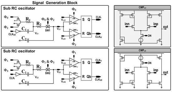
Figure 11. The circuit diagram of the signal generation block.
A transmission gate switch, SW1 (or SW2), is positioned between R2 and VO1 (or VO2). Without this switch, the output voltage would continue to vary, even when the phase changes due to the voltage difference between the output voltage and VC1. Therefore, the switches prevent voltage changes during the comparison period for the reference generation. Additionally, given the presence of a parasitic diode at the drain of the switch transistor, it is important to control the voltage swing to prevent forward biasing to the diode. This ensures the diode does not conduct unintentionally, maintaining the integrity and performance of the switch. The comparators are turned on only for one of the four phases when they need to be used for comparison, reducing 75% of the comparators’ dynamic power consumption.
3.2. Reference Voltage Generation
Figure 12 shows a detailed circuit diagram of the reference voltage generation block. A resistor divider generates the reference voltage, VUP and VDN, for the voltage swing of VO1 and VO2. VUP and VDN determine the up and down stop voltage, respectively. To compensate for the temperature variation in the resistor in the sub RC oscillator, the reference voltages are generated by the voltage divider using different types of resistors (p-poly and n-well) with opposite temperature coefficients. The Gm amplifiers process the voltage error and update the reference voltages, VLU1, VLU2, VLD1 and VLD2. VO1 is sampled at phases Ф1 and Ф3, and VO2 is sampled at phases Ф0 and Ф2. During the sampling period, the Gm amplifier compensates for any voltage swing errors by adjusting the output. It compares the actual swing (VO1, VO2) to the target values: VUP when the swing rises and VDN when the swing falls. It helps the voltage swings remain within VUP − VDN, resulting in the overall suppression of the offset voltage and 1/f noise of the comparators and the Gm amplifiers [7]. The Gm amplifier is employed to minimize the voltage ripple of the reference voltages during updates. The Gm amplifier uses chopped output, and the output voltages are unpredictable due to its high impedance output. When the switch is on, a charge-sharing phenomenon between the reference voltage capacitor and the amplifier output capacitor occurs, leading to a voltage ripple. This ripple has the potential to degrade the noise performance, so the sub-amplifiers are critical in mitigating this effect and maintaining a stable and clean output. Therefore, the sub-amplifiers with extra switches driven by Ф0 or Ф2 are designed to set the Gm amplifier output to be the near voltage of the reference voltage before updating occurs. This preset helps to minimize the voltage ripple, ensuring a smoother and more accurate reference voltage update.
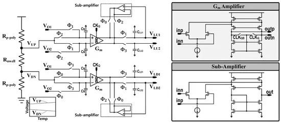
Figure 12. The circuit diagram of the reference voltage generation block.
4. Measurement
The proposed oscillator was implemented with 0.18 μm CMOS technology in an active area of 0.067 mm2. The oscillator generates 469.2 kHz with the distributed RC network where R1, R2, C1 and C2 are chosen to 204 kΩ, 408 kΩ, 654 fF and 327 fF, respectively, and consumes 23.4 μW at a supply voltage of 1.8 V. Figure 13 presents a microphotograph of the proposed distributed RC oscillator chip.
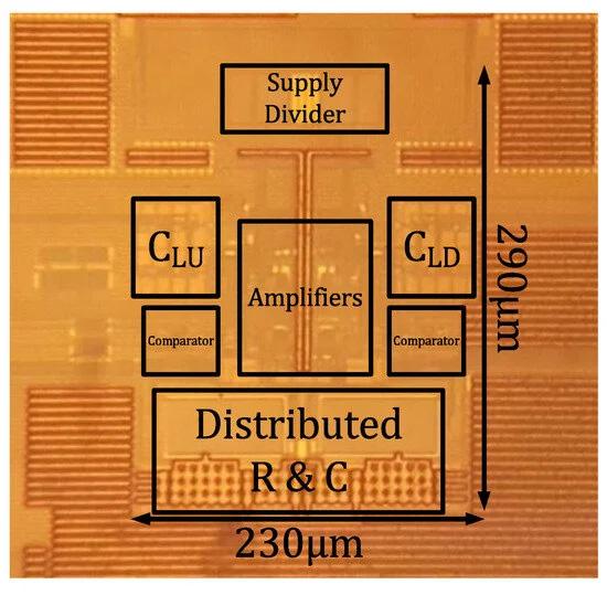
Figure 13. Chip photo.
Noise Measurement
Figure 14 shows the measured phase noise of the proposed distributed RC oscillator, with an oscillation frequency of 469.2 kHz. The measurements indicate phase noise levels of −70.35 dBc/Hz, −88.64 dBc/Hz, −108.33 dBc/Hz and −122.92 dBc/Hz at offsets of 100 Hz, 1 kHz, 10 kHz and 100 kHz, respectively.
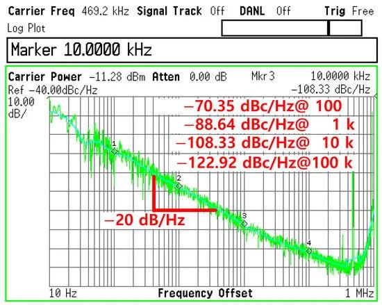
Figure 14. Measured phase noise.
Figure 15 shows the measured jitter of the output clock signal. The jitter histogram hits 1.2 million counts, and it shows that the peak-to-peak jitter is 3.9 ns and the RMS jitter is 571.6 ps. Given the oscillation frequency of 469.2 kHz, the jitter constitutes 0.0268% of one complete clock period.

Figure 15. Measured jitter.
Figure 16 shows the measured Allan deviation which shows the long-term stability of the clock signal. It indicates that the clock can maintain a variation of 0.7 ppm up to 100 s.

Figure 16. Measured Allan deviation.
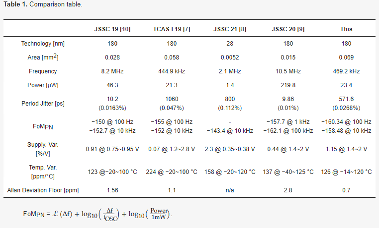
Table 1 provides the comparison results among the recent relaxation oscillator papers that measured the phase noise. It shows that the proposed oscillator can improve the noise performance compared to those proposed in the previous papers.
Table 1. Comparison table.
5. Discussion
In this study, we have presented a comprehensive design and implementation of a distributed RC oscillator aimed at improving the noise performance and frequency stability of RC oscillators, which can be used in compact devices. Our proposed two-stage distributed RC network effectively enhances the signal transition slope at the comparator input, which is a critical factor in improving the noise performance of RC oscillators. A significant noise performance improvement could be achieved by maximizing the transition slope with a phase shift close to −π.
Expanding the RC network to additional stages increases the transient slope and may further improve the noise performance, but it also presents considerable challenges. Critical concerns include issues like the voltage swing dipping below ground level and the increased area requirement in proportion to the number of stages. Future research could concentrate on refining the design to mitigate these downsides while preserving the advantages offered by multiple stages.
Various resistor and capacitor sizing strategies emphasize optimizing these components to improve the quality factor, Q. It appears feasible to achieve a larger Q by opting for a larger R2 compared to R1 and a smaller C2 relative to C1. Additionally, the measurement outcomes from the implemented oscillator indicate its potential to attain low-phase noise and high-frequency stability.
6. Conclusions
This research has effectively shown the design strategy of a two-stage distributed RC oscillator, marking a substantial progression in noise performance and frequency stability. By innovatively enhancing the signal transition slope and carefully fine-tuning the resistor and capacitor values, the impact of comparator noise can be significantly reduced, and it improves the overall system efficiency. Adopting a quadrature oscillator topology and refined reference voltage generation methods further improve the oscillator’s reliability and precision. The implemented RC oscillator, fabricated in 180 nm CMOS, provides a stable frequency of 469.2 kHz while consuming 23.4 μW at a supply voltage of 1.8 V. It also achieves a FoM of −160 dBc/Hz at 100 Hz and an Allan deviation floor of less than 0.6 ppm. Although there are challenges inherent to multiple stages, the oscillator exhibited encouraging results, including low-phase noise and high-frequency stability, demonstrating its potential for broad use in precision-critical environments. Future work will refine the design to address existing challenges, explore advanced noise-reducing techniques and integrate the oscillator into diverse applications. The findings of this study provide a robust basis for the future development of more efficient, precise, and compact RC oscillators, propelling advancements in frequency generation technologies.