
Abstract
To solve the problems of large switching losses and the need for large-capacity electrolytic capacitances in three-phase DC/AC on-board chargers for vehicle-to-grid (V2G) applications, this paper proposes a single-stage bidirectional high-frequency isolated converter that eliminates the need for large-capacity capacitances. Combined with the proposed modulation scheme, it can theoretically reduce the switching loss by about two-thirds with the three-phase converter compared with the conventional modulation scheme, improving the converter’s operating efficiency and power density. Firstly, based on the characteristics of the proposed topology, a hybrid modulation scheme is proposed, which combines a phase-shift modulation scheme based on double modulation waves and a sawtooth carrier with a 1/3 modulation scheme, and the theoretical feasibility of the hybrid modulation scheme is verified using a mathematical modeling equation. Secondly, this paper provides a detailed analysis of the four operating modes of the two full-bridge circuits and the commutation process of the three-phase converter within 1/6 of the fundamental frequency cycle (P1 modulation interval). Then, the control strategy is given for the constant-current and constant-voltage charging and constant-current discharging for electric vehicle batteries. Finally, simulation results verify the correctness of the proposed topology and modulation scheme in vehicle–grid interaction.
Keywords: isolated bidirectional DC/AC converter; single stage; hybrid modulation scheme; high power factor; low loss; V2G
1. Introduction
V2G technology enables the interaction between electric vehicles and the power grid, employing intelligent scheduling to manage the orderly charging and discharging of electric vehicles. This approach achieves peak shaving and valley filling and improves the efficiency of power grid operation [1,2,3]. In recent years, the research and development of electric vehicles have witnessed a prominent trend in the emergence of 800 V electric vehicle charging and discharging platforms that utilize V2G technology [4,5,6].
The 800 V electric vehicle charging and discharging platform based on V2G technology has been a new trend in the research and development of electric vehicles over recent years. This innovative approach significantly enhances the charging and driving performance of electric vehicles, thus attracting widespread attention from researchers. In constructing high-power electric vehicle charging and discharging platforms, the power density and operational efficiency of the converter, as the central power conversion device, assume crucial status [7,8,9]. In recent years, single-phase bidirectional DC/AC converters have found extensive application in both on-board and off-board charger construction [10,11,12]. However, they encounter challenges in meeting the demanding criteria of high power transmission capacity and achieving three-phase balanced charging and discharging within the charging and discharging system. A three-phase bidirectional DC/AC converter plays a crucial role in ensuring a balanced voltage and avoiding burdening the power grid [13,14]. However, traditional dual-stage line-frequency isolated three-phase converters have a large volume, high costs, high levels of noise pollution, and the necessity for electrolytic capacitances between the stages, which is challenging to apply to in-vehicle environments. An alternative dual-stage high-frequency isolation approach utilizing a high-frequency transformer (HFT) in place of a line-frequency transformer offers improved power density and operational efficiency [15,16]. Still, it requires a large-capacity capacitance to maintain the stability of the intermediate DC link, which not only increases the system cost but also affects the converter’s operational efficiency.
In response to these challenges, researchers have explored various topologies to enhance transformation efficiency and power density [17,18,19]. Refs. [20,21] introduce a cycloconverter known for its high power density and bidirectional energy flow capability; however, it suffers from significant voltage spikes that compromise its safe operation. Even with the incorporation of buffer circuits and an enhanced control strategy, this approach still adds complexity to the system and complicates the implementation process [22]. In [23], a single-stage three-phase converter with high-frequency isolation and power correction is investigated. This converter supports bidirectional power flow and finds applications in DC power grids, electric vehicles, and various other fields. Nevertheless, the excessive deployment of switching devices and an intricate control strategy diminish both the operational efficiency and system reliability of the converter.
Furthermore, refs. [24,25,26] enhance operational efficiency through the adoption of soft switching technology and the alteration of modulation schemes. In [24], soft switching technology is employed to mitigate the switching loss in three-phase inverters. However, this approach necessitates the incorporation of extra switching devices, passive components, and auxiliary circuits, leading to increased system costs and complexity. To minimize switching loss without introducing additional components or auxiliary circuits, refs. [25,26] employ an advanced modulation scheme. This scheme replaces the high-frequency mode of the switching transistor with a stable state through pulse width modulation, resulting in a one-third reduction in the average switching frequency and consequently lowering the switching loss. In [27,28], although the hybrid modulation strategy reduces 2/3 of the switching loss on partial topology, it increases the switching devices and structural redundancy. Consequently, this paper presents a single-stage, bidirectional high-frequency isolated three-phase DC/AC converter. This converter boasts single-stage direct power conversion, the absence of an intermediate electrolytic capacitance, compact transformer dimensions, and minimal switching loss.
The rest of this paper is organized as follows: The proposed topology structure and modulation scheme are introduced in Section 2, and the establishment of the relevant mathematical models and analysis of theoretical losses are mentioned. In Section 3, a detailed analysis of the proposed converter is presented, which helps to understand the working principles. In Section 4, the control strategy is analyzed to be applicable to the on-board charger during battery charging and discharging. A simulation is conducted in Section 5 for validation of the proposed power conversion system and control strategy; it conducts a comprehensive analysis of the two control modes for electric vehicle battery charging and discharging within the V2G context. In addition, simulations are carried out in programs that resemble experimentation in PSIM to better verify the bidirectional power flow and effectiveness of the topology. A discussion in Section 6 analyzes and summarizes the results obtained, and provides possible direction for future research. Conclusions are drawn and the limitations of the proposed topology are analyzed in Section 7.
2. Analysis of Topology Structure and Modulation Scheme of the Proposed Converter
2.1. Topology Description
Figure 1 illustrates the proposed single-stage bidirectional high-frequency isolated three-phase DC/AC converter topology in this paper. The primary full bridge (Q1–Q4) is interconnected with the secondary full bridge (S1–S4) via the leakage inductance Lr and HFT, which facilitates the voltage transformation and electrical isolation. The secondary-side three-phase converter (T1–T6) connects to the secondary full bridge on one end and to the filter inductances Lf and filter capacitances Cf on the other end before its final connection to the grid. The DC side is characterized by voltage Vdc and current Idc. V1 and V2, i1 and i2 represent the voltage and current on the primary and secondary sides of HFT, respectively, with HFT’s ratio denoted as n (n = 1). Vlink refers to the high-frequency pulse-width voltage of the secondary full-bridge output, while ia, ib, ic and Va, Vb, Vc represent the three-phase phase currents and phase voltages on the grid side.

Figure 1. The single-stage bidirectional isolated three-phase DC/AC converter topology.
Both full-bridge circuits operate in a bidirectional phase-shift mode, generating a high-frequency six-pulse pulsating waveform. The three-phase converter on the secondary side is modulated to transform the positive high-frequency pulsating square wave voltage into balanced three-phase sinusoidal voltages through filtering. Subsequently, the output voltage is linked to the grid, achieving DC/AC sine wave conversion. In contrast to the dual-stage bidirectional isolated DC/AC converter, which utilizes a large capacitance, the proposed single-stage DC/AC topology eliminates the need for a DC link. This enables direct power transfer between DC and three-phase AC, resulting in an enhanced converter lifespan and operational efficiency.
2.2. Hybrid Modulation Scheme
Figure 2 depicts a modulation scheme featuring dual modulation waves and a sawtooth carrier, which builds upon the isolated phase-shifted full-bridge modulation scheme and the cycloconverter modulation scheme. GQ1–GQ4 and GS1–GS4 correspond to the driving signals for the respective Insulated Gate Bipolar Transistors (IGBTs). dp and dn denote the modulation waves for the leading and lagging bridge arms within the primary full bridge, respectively. V1 and V2 represent the high-frequency pulse-width voltages on the primary and secondary sides of HFT. Vc signifies the sawtooth carrier wave, with the switching cycle Ts for each IGBT being twice the carrier cycle Tc. Lastly, Vref represents the reference modulation wave for the primary full bridge, derived by obtaining the absolute value of the three-phase line voltage at its maximum, and its frequency (300 Hz) is six times that of the sinusoidal AC line voltage.
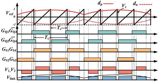
Figure 2. Full-bridge circuit-switch timing diagram.
An on-state signal is generated when Vc exceeds Vref, and conversely, when Vc exceeds Vref again, the driving signal is inverted to produce an off-state signal. Q1 and Q4 being in the on-state result in a positive high-frequency voltage on the primary side of HFT. Conversely, the on-state of Q2 and Q3 leads to a negative high-frequency voltage on the primary side of HFT. When either Q1 and Q2 or Q3 and Q4 are simultaneously on, the voltage on both the primary and secondary sides of HFT becomes zero. Q1(Q3) and Q2(Q4) are sequentially turned on, creating a phase shift angle α between Q1 and Q2. The output three-phase line voltage can be linearly adjusted by varying α, which is determined by Vref. Assuming m represents the amplitude of Vref, dp and dn can be expressed as (1).
⎧⎩⎨????p=????????n=−????????=????????ref(1)
When S1 and S4 are turned on, S2 and S3 are turned off; when S2 and S3 are turned on, S1 and S4 are turned off. The secondary side full-bridge circuit’s IGBTs consistently operate at a 50% duty cycle. S1 and S4 are switched on only when Q1 and Q2 are switched on, and off when Q3 and Q4 are switched on. Conversely, S2 and S3 are switched on only when Q3 and Q4 are switched on, and off when Q1 and Q2 are switched on. Therefore, the secondary full bridge can generate unipolar high-frequency pulse-width voltage with the characteristics of a six-pulse waveform.
To demodulate the high-frequency pulse-width voltage waveform into a three-phase sinusoidal voltage waveform, modulation of the three-phase converter on the secondary side is required, and a 1/3 modulation scheme is proposed. Since Vref is a six-pulse waveform, a fundamental frequency cycle can be divided into six equal modulation intervals (P1–P6) for analysis. Figure 3 illustrates the corresponding waveforms of the 1/3 modulation scheme. Mod-A, Mod-B, and Mod-C represent the reference modulation waveforms for the A-phase, B-phase, and C-phase bridge arms, respectively. GT1–GT6 represent the driving signals for T1–T6.

Figure 3. Key waveforms of 1/3 modulation scheme.
During each modulation interval, a single bridge arm engages in high-frequency switching while the other two maintain a steady state at either a high or low level. It can be inferred that within a fundamental frequency cycle, each IGBT in a three-phase converter operates in a high-frequency switching state for one-third of the cycle. Table 1 illustrates the switching states of T1–T6 during each modulation interval.
Figure 4 illustrates a phase-shift modulation scheme using dual modulation waves and a sawtooth carrier, integrated with 1/3 modulation to create a hybrid modulation approach for the converter proposed in this paper. This scheme primarily enables direct power transmission from the DC to the AC side, as depicted in Figure 4. It is important to note that this converter design supports bidirectional power conversion, allowing for power flow from the AC to the DC side.

Figure 4. Overall hybrid modulation scheme.
2.3. Loss Analysis
The analysis indicates that in a three-phase converter on the secondary side, all IGBTs are in a high-frequency switching state for only one-third of the fundamental frequency cycle. This design effectively reduces switching loss, and the loss of converters with different topologies mainly includes on-state loss and switching loss. The on-state loss (Pcon) of IGBTs under different modulation schemes can be calculated using the following equation:
(2)
Here, m represents the adjustment factor, Ic is the collector current, Vce is the on-state voltage drop between the IGBT collector and emitter, and rfd is the on-state resistance. Under identical operating conditions, the on-state loss of the converter remains approximately consistent across different modulation schemes. The equation to calculate the switching loss (Pswi) of IGBTs is given as follows.
(3)
In this context, Vlink represents the input voltage of the three-phase converter during IGBTs’ opening and closing phases. ton and toff represent the respective opening and closing times of the IGBTs, while Ts is the switching cycle time. Additionally, fi(θ) is a function related to the high-frequency switching current. Under identical working conditions, the frequency of IGBT switching directly impacts the switching loss. The three-phase converter employs a constant DC link square wave control combined with sine pulse width modulation (SPWM). The total switching loss can be expressed as (4).
(4)
Psw,DPWMMIN represents the total switching loss of the high-frequency isolated three-phase converter, which uses 180° square wave control and a discretized pulse width modulation scheme based on minimum switching loss (DPWMMIN). Psw,ADPWM represents the total switching loss of the three-phase converter using the hybrid modulation scheme proposed in this paper.
(5)
The proposed scheme in this paper minimizes switching loss, effectively reducing both the average switching frequency and switching loss. This aligns with the theoretical predictions.
2.4. Mathematics Modeling
Taking the inversion process as an example, the feasibility of the proposed hybrid modulation scheme is analyzed through mathematical modeling. The rectification process follows the same approach. The reference modulation wave of the primary side full-bridge circuit is a six-pulse Vref(t), where one fundamental cycle is divided into six modulation intervals, as expressed in (6).
(6)
Taking the P1 modulation interval as an example, a double fourier analysis is performed on the high-frequency pulse width voltage Vlink, resulting in the extraction of the fundamental component of Vlink as (7).
(7)
In (7), m represents the modulation ratio, with a value range of 0 ≤ m ≤ 1. Similarly, for the P2 modulation interval, Vlink is expressed as (8).
(8)
If the switch states of the bridge arms for phase A, phase B, and phase C of the three-phase converter on the secondary side are denoted as Sa, Sb, and Sc, respectively, then
(9)
Let the neutral point voltage be represented as eo, and express Kirchhoff’s Voltage Law equation for the three-phase converter on the secondary side as follows.
(10)
In (10), pairwise subtraction is applied, resulting in expression for the line voltage on the grid side as (11).
(11)
The expression for the IGBT states in the P1 modulation interval is as (12).
(12)
When the harmonic components are not considered, substituting (12) into (11) will result in three-phase line voltages on the grid side as (13).
(13)
From (13), the grid-side line voltages are three-phase sine voltages. By repeating the operation of the above equation, the expression of the three-phase line voltages obtained in the P2–P6 modulation intervals is consistent with (13). Therefore, it can be proven that the proposed hybrid modulation scheme is feasible.
3. Operating Process and Mechanism of the Converter
3.1. Operating Principle of Two Full-Bridge Circuits
To simplify the analysis, the following assumptions are made. Assuming that all IGBTs, inductances, and capacitances are ideal, that is, the parasitic capacitance of all IGBTs (Q1–Q4, S1–S4, T1–T6) is ignored, and there is no loss in the inductances and capacitances. Assuming that the current commutation process is very rapid, it can be considered to be completed instantly, and the voltage ratio of HFT is 1. The leakage inductance Lr of HFT is equivalent to the primary side of the ideal transformer.
There are a total of eight operating modes in a complete switching cycle of two full-bridge circuits of the converter. Due to the symmetry between the last four operating modes and the first four, in order to avoid lengthy repetition, this paper only analyzes the first four operating modes. In addition, only analyzing the buck operating mode, the analysis of the boost operating mode is similar. The first four modes are described in detail below Figure 5, and graphic representations of such modes are presented in Figure 6.

Figure 5. Operating modes of the full-bridge circuit: (a) mode 1; (b) mode 2; (c) mode 3; (d) mode 4.

Figure 6. The theoretical waveforms of the full-bridge circuit in buck mode.
Mode 1: [t0–t1, Figure 5a] Q1 and Q4 are on simultaneously, while i1 flows through Q1, the primary winding, and Q4 in sequence. On the secondary side of HFT, S1 and S4 are both in the on-state, S2 and S3 are both in the off-state, and i2 only flows through the anti-parallel diodes of S1 and S4. V1 and V2 are equal to Vdc, and the output voltage Vlink of the full-bridge circuit on the secondary side is equal to Vdc.
Mode 2: [t1–t2, Figure 5b] At t1, Q1 is turned off. i1 commutates from Q1 to the anti-parallel diode of Q3, V1 and V2 become 0, and the primary side of the HFT is in a freewheeling state, so the zero voltage switching (ZVS) of Q3 can be realized. There is no clamping voltage on the secondary side, and all S1–S4 are turned on. The current on the secondary side is also in a circulating state and linearly decreases.
Mode 3: [t2–t3, Figure 5c] At t2, Q4 is turned off. i1 flows through the anti-parallel diodes of Q2 and Q3, and the ZVS of Q2 can be realized. The operating process on the secondary side is similar to Mode 2. In addition, Vdc is applied at both ends of Lr, V1 changes from 0 to −Vdc, but V2 remains at 0, with no power transmitted to the secondary side, resulting in duty cycle loss. In this mode, the energy stored in Lr is transmitted back to the DC side, and i1 and i2 rapidly decrease linearly. The expression for i1 is as follows.
Mode 4: [t3–t4, Figure 5d] At t3, i1 decreases in the forward direction to 0, and i1 commutates from the anti-parallel diodes of Q2 and Q3 to Q2 and Q3. Due to the discharge of capacitance C, both i1 and i2 begin to rapidly increase in reverse, and the expression for i1 is as (16).
At t4, mode 4 ends and the i2 freewheeling state ends. i2 flows through the anti-parallel diodes of S2 and S3, while the anti-parallel diodes of S1 and S4 naturally are turned off. At this point, V1 and V2 are equal to −Vdc, and the duty cycle loss process ends.
3.2. Operating Principle of Three-Phase Converter on the Secondary Side
The commutation process of the three-phase converter in the P1 modulation interval is shown in Figure 7, Figure 8 and Figure 9. In the P1 modulation interval, T4 and T5 are normally on, T3 and T6 are normally off, and T1 and T2 are in a high-frequency modulation state, with a total of three cases. Given that the switching function of T1 is Sa1, and the switching function of T2 is Sa2, so Sa1 + Sa2 = 1.

Figure 7. Case 1.

Figure 8. Case 2.

Figure 9. Case 3.
As shown in case 1 of Figure 7, T1 is in a high-frequency switching state and T4 is normally on. When T1 is turned on, VRY is equal to Vlink; when T1 is turned off, VRY is equal to 0. VRY can be expressed using (17).
As shown in case 2 of Figure 8, both T4 and T5 are normally on, so VYB can be expressed using (18).
As shown in case 3 of Figure 9, T2 is in a high-frequency switching state, and T5 is normally on. When T2 is turned on, VBR is equal to Vlink; when T2 is turned off, VBR is equal to 0. VBR can be expressed using (19).
Therefore, the high-frequency pulse width line voltages VRY, VYB, and VBR can be transformed into grid line voltages Vab, Vbc, and Vca after being filtered by LC filters. The analysis of the remaining modulation intervals is similar and will not be repeated here.
4. Control Strategy
4.1. Charging and Discharging Control Strategy
Figure 10 shows the closed-loop control of the converter, consisting of outer-loop control for battery charging and discharging and inner-loop control for the current on the grid side.

Figure 10. Charging and discharging control strategy.
Battery charging and discharging control encompasses managing both current and voltage levels. To optimize battery lifespan and efficiency, the charging process employs a two-stage approach, initially using a constant current and transitioning to a constant voltage. Initially, a constant current is applied to charge the battery. Once the specified state of charge (SOC) threshold is reached, the current controller disengages and the voltage controller takes over, maintaining a constant-voltage charging state. This two-stage charging method mitigates the issues of overcurrent during the initial phase and inadequate current during constant-voltage charging, as well as preventing overcharging during the later stages of constant-current charging. Furthermore, the switching module within the charging and discharging system enables flexible transitions between battery charging and discharging states.
The battery discharging process utilizes a constant-current method, ensuring consistent current output from the battery. Simultaneously, it guarantees that the discharge current remains within acceptable limits while supplying energy to the grid rapidly. The control system is implemented in the dq coordinate system and employs a proportional–integral (PI) controller. The reference current, determined by the battery voltage or current controller, serves as the reference for the active current on the grid side. To ensure the unit power factor operation of the converter, the reference value for the reactive current on the grid side is set to 0. The specific control equation is provided below.
In (20) and (21), Kvp and Kip represent proportional coefficients, while Kvi and Kii represent integral coefficients. Vdc,ref, Idc,ref, id,ref, iq,ref serve as reference values for Vdc, Idc, id, and iq, respectively. Grid-side current control employs an inner-loop current control system utilizing a feedforward decoupling method to achieve independent control of id and iq. Much like the outer-loop control of battery voltage or current, the inner-loop current control predominantly employs a PI controller, with the specific control equation given below.
In (23), kip represents the proportional coefficient, and kii represents the integral coefficient. Vd and Vq are the dq components of the grid-side voltages, while id and iq correspond to the dq components of the grid-side currents. Observing Figure 10, it is evident that the control strategy involves synchronizing with the phase of the grid-side voltages. To fulfill the requirements of the six-pulse wave modulation scheme, the reference modulation waveform generated using this scheme must be transformed into a line component.
4.2. Phase Adjustment of the Encoded Signals in the MUX
The reference line voltage employed in the hybrid modulation scheme mentioned earlier is derived from (24) and is specified with φ = 0°, indicating that the initial phase is set to 0 as a fundamental condition. Since the actual grid line voltage may not have an initial phase of zero, the reference modulation wave generated by the control strategy will also have a non-zero initial phase (i.e., φ ≠ 0°), resulting in a phase shift in the modulation waves for each modulation interval compared to the original modulation waves.
Therefore, it becomes essential to align the phase of the encoded signal in the MUX with the initial phase of the actual grid line voltage. Initially, the control strategy samples the initial phase of the reference modulation wave and compares it with the zero phase to determine the phase difference. Subsequently, this phase difference is transformed into a time offset signal and incorporated into the encoded signals from signal1 to signal6.
This ensures that the modulation states of T1–T6 align with each modulation interval. The flowchart illustrating the phase adjustment control strategy is depicted in Figure 11.
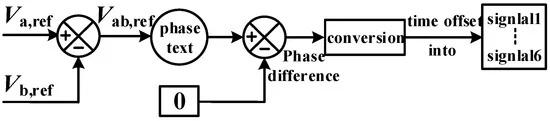
Figure 12 presents the simulation results of charging and discharging. During 0.1 s–1.6 s, there is a two-stage constant-current–constant-voltage charging process. In Figure 13, the alternating current is sinusoidal and symmetrical, with a 180° phase difference between voltage and current, achieving unity power factor operation. During 0.1 s–0.8 s, the battery is in the constant-current charging region. The charging current remains constant at −30 A during this time, resulting in a gradual increase in the battery voltage and SOC. When t = 0.8 s is reached, the battery SOC reaches the preset value of 80%, entering the battery’s constant-voltage charging region. The battery terminal voltage remains constant at 659 V while the charging current gradually decreases, resulting in a further increase in the battery SOC.
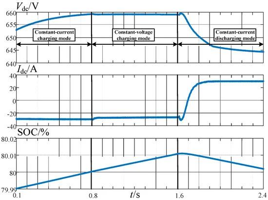
Figure 12. Charging and discharging modes.
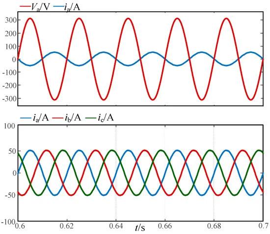
Figure 13. Grid-side currents and voltages.
At t = 1.6 s, the battery enters the constant-current discharge region. At this point, the grid-side current is sinusoidal and symmetrical, voltage and current are in phase, with a power factor of 0.999, and the battery releases energy with a high-power factor into the grid. The constant-current discharge region is set to maintain a constant current of 30 A. During this period, the battery voltage gradually decreases, and the battery SOC decreases accordingly. During the dynamic process of battery charging and discharging, the charging current and voltage quickly follow the set values, and the switching process occurs smoothly and stably. This indicates that the converter can achieve bidirectional energy transfer with a unity power factor and exhibits a good transient response, demonstrating the feasibility of the proposed battery charging and discharging control strategy.
Harmonic analysis of grid-side AC current under both battery charging and discharging states is conducted, as shown in Figure 14a,b. The distortion rate of grid-side current during charging is 1.03%, while it is 1.69% during discharging. The grid-side current distortion is relatively low, complying with grid connection standards.
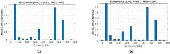
Figure 14. Analysis of grid-side current distortion: (a) FFT of grid-side charging current; (b) FFT of grid-side discharging current.
Figure 15 illustrates the primary-side voltage V1 and the high-frequency pulse-width voltage Vlink output from the secondary-side full-bridge circuit. The waveform of current i2 is consistent with the analysis of various operating modes presented in Figure 6.
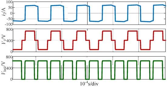
Figure 15. Waveforms of i1, V1, and Vlink.
Figure 16 shows the reference modulation wave Vref of the primary-side full-bridge circuit, the reference modulation waves Mod-A, Mod-B, Mod-C of the secondary-side three-phase converter, and their driving signals GT1, GT3, GT5. The simulated waveforms align with the analysis presented in the previous section on hybrid modulation, demonstrating that the IGBTs of the proposed converter operate in a high-frequency modulation state only during 1/3 of the fundamental frequency cycle.
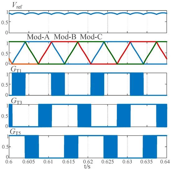
Figure 16. Key waveforms during the modulation process of three-phase converter.
The simulation results validate the feasibility of the converter topology and the proposed hybrid modulation scheme in the context of electric vehicle battery charging and discharging scenarios.
Figure 17a,b verifies the correctness of the converter in the inverter state. The DC-side voltage is 600 V, with a modulation ratio of 0.9, and resistance load value under full load on the AC side of 8.06 Ω, and a rated power set to 18 kW. Figure 17a shows the voltage and current waveforms of phase A. Figure 17b shows the three-phase voltage output by the converter with a resistive load on the AC side. Figure 17c verifies the correctness of the converter in the rectified state. The AC-side phase voltage is 220 V, with a modulation ratio of 0.9. Figure 17c shows the DC-side voltage.
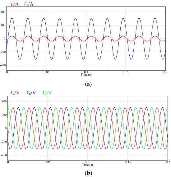
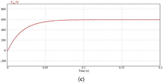
Figure 17. Analysis of bidirectional power flow: (a) voltage and current waveforms of phase A; (b) three-phase output voltages; (c) DC-side voltage.
The waveforms representing the port characteristics and modulation characteristics are shown in Figure 18. Furthermore, we simulate the efficiency of the inverter when the AC side of the converter is a resistive load. For example, the light load operation is represented by 20 percent of rated power (18 kW) here, indicating that the proposed converter’s output power is 3.6 kW. The values of the resistance load under light- and full-load condition are 40.33 Ω and 8.06 Ω, respectively. Figure 19 shows the variation of PSIM experimental efficiency with the load for the presented converter. The maximum efficiency achieved in the experimental 18 kW prototype in PSIM is 94.45%.
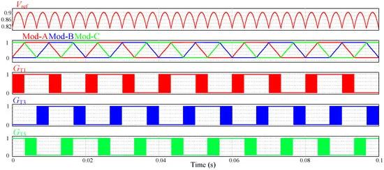
Figure 18. Important verification waveforms.
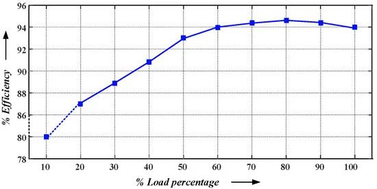
Figure 19. Variation of 18 kW converter efficiency with load.
The above simulation results are consistent with the theoretical analysis, which verifies the correctness of the proposed modulation scheme.
6. Discussion
In the Simulink simulation, the scenario of charging and discharging electric vehicle batteries using the constant-voltage and -current methods is simulated. The dynamic performance of battery voltage and current is good, and the target value could be quickly tracked. The results indicate that the converter has greater potential in V2G power conversion. In addition, regarding the modulation characteristics of the converter, simulation results show that compared to SPWM modulation and other types of modulation, the proposed converter with hybrid modulation scheme reduces the average switching frequency and reduces switching losses.
In a PSIM simulation that resembles the experimental environment, the rectification and inversion of the converter are verified, and the efficiency of the converter under inversion is verified under a rated load of 18 kw on the grid side, fully demonstrating the correctness of the converter.
Looking ahead, our future work will focus on exploring advancements in our approach. In future work, a system with supply voltage asymmetry should be considered. Because the actual power grid is not in an ideal state, the proposed converter should overcome power supply voltage imbalance and be more suitable for V2G or other application scenarios. In addition, in order to improve the power density and reduce the waveform distortion rate, and to be better applicable to more scenarios, a control strategy for related harmonic suppression is also the next step from this paper. Finally, we will explore the use of the proposed converter in more scenarios, such as, three-phase uninterruptible power supply in an islanded or standalone microgrid.
7. Conclusions
This paper offers a comprehensive analysis covering modeling derivation, operating principles, a hybrid modulation scheme, battery charging and discharging control strategies, as well as simulation verification for the proposed single-stage high-frequency isolated three-phase bidirectional DC/AC converter topology. In the context of V2G applications, the proposed converter topology and control strategy exhibit the following benefits:
Firstly, the proposed converter utilizes a single-stage topology structure, eliminating the need for an intermediate DC link and enabling genuine direct power transmission. In contrast to the conventional isolated two-stage charging and discharging topology, it offers superior power density and efficiency, making it suitable for vehicle–grid applications.
Secondly, the linear and straightforward relationship between the output voltage and modulation ratio allows for power conversion through a straightforward hybrid modulation scheme, making it highly practical for engineering applications.
Finally, within a single fundamental frequency cycle, each IGBT in the three-phase converter operates in a high-frequency modulation state for just 1/3 of the cycle, maintaining a stable state for the remaining 2/3. This approach minimizes switching loss and enhances the overall operational efficiency of the converter.
However, the proposed topology also has shortcomings for managing energy flows. The application of the proposed converter in high-power conversion scenarios poses challenges. The Vlink is very high, which will affect the operation of IGBT and may generate voltage spikes. In practice, high-power conversion will bring serious waveform distortion and unstable factors to the power grid. This converter is currently suitable for a system with supply voltage symmetry, and application in asymmetric systems remains a challenge.