Abstract
Event cameras are bio-inspired devices that have revolutionized the acquisition of visual information by mimicking the neural architecture of the eye. These cameras respond asynchronously to changes in scene illumination at the pixel level, providing high-precision time information with low latency, typically in the order of microseconds. In this work, we experimentally evaluate an optical camera communication (OCC) link using an LED-based transmitter and an event camera as the receiver. We propose n-pulse modulation to encode data, adapting the system to the specific characteristics andoperational principles of event cameras. The proposed scheme significantly reduces the demodulation complexity compared to other alternatives found in the literature. Furthermore, a set of experiments considering different camera bias sensitivities, encoding duty cycles, and LED radiant fluxes were carried out. The results showed that the BER performance was strongly dependent on the received optical power and the bias sensitivity. In addition, duty cycles between 0.3 and 0.7 at a 200 Hz transmission frequency presented the best performance, with a BER below 1.25×10⁻⁴">1.25×10−41.25×10−4, which is under the forward error correction (FEC) limit. This work showcases the cutting-edge capabilities of event-camera-based OCC technology and contributes to the ongoing revolution in optical wireless communication (OWC).
1. Introduction
The exponential proliferation of wireless devices relying on radio frequency (RF) signals for communication, coupled with the increase in demanding fast data rate applications, has resulted in the saturation of the shared spectrum and bandwidth scarcity. In response to these issues, the use of higher frequency bands, including millimeter waves and terahertz, has emerged as a complementary solution. The current 5G definition considers the use of higher frequency bands around 24.1–27.8 GHz, and it is planned to also utilize the 40 GHz and 60 GHz frequencies in the near future [1,2]. Above the terahertz spectrum, optical wireless communication (OWC), operating from 350 to 1550 nm (spanning from ultraviolet to mid-infrared bands), has emerged as a potential solution for mitigating the challenges posed by the escalating demand for bandwidth and communication resources [3].
Traditional OWC-based technologies such as light-fidelity (LiFi) and visible light communication (VLC) target applications in which high to very-high data rates are needed [4]. On the other hand, optical camera communication (OCC) is a subtype of optical wireless communication (OWC) technology that utilizes image sensors as receivers operating in either the infrared (IR) or visible bands. In comparison to other OWC technologies, OCC presents several advantages. First, it allows the use of current component-off-the-shelf cameras present in many devices as receivers, without additional adaptation. Second, these devices offer inherent spatial division multiplexing (SDMA) capabilities thanks to the use of image-forming optics and a large number of pixels. As a result, OCC-enabled devices can simultaneously collect information from a massive number of endpoints, making them suitable for communication and various other applications. This latter feature fits into one of the joint communication and sensing (JC&S) paradigms of 6G, which integrates sensing and communications operations on a single piece of hardware, while using the same spectral resources [5].
Due to its cost-effectiveness and highly aggregated information-carrying capability, OCC has garnered significant attention in indoor and outdoor domains, including for intelligent transportation and positioning systems [6], underwater communication [7], and IoT connectivity [8]. While OCC appears to be a promising solution for addressing challenges in wireless communication systems, it presents some limitations. These include, but are not limited to, a low data rate resulting from the receiver’s low sampling rate, reduced dynamic range, high power consumption, and large latency [9].
The latest advancements in alternative camera technologies, such as event, multispectral, hyperspectral, and thermal, have opened up new possibilities in the field of OCC. The bio-inspired technology of “silicon retinas”, proposed in [10], mimics the neural architecture of the eye, introducing a new philosophy on how visual information can be gathered. These “silicon retinas”, which have received other nomenclatures such as event-based cameras or dynamic vision sensors (DVS), respond asynchronously to scene illumination variations at the pixel level, offering high-precision time information and low latency (both in the order of microseconds). In contrast, conventional cameras typically acquire absolute intensity image frames at fixed time intervals. DVS devices measure pixel-wise brightness changes asynchronously rather than measuring absolute brightness at a constant rate [11]. Since DVS presents a sparse, fast, and highly dynamic range output, they can overcome the limitations of frame-based cameras [12]. In this study, an optical communication system utilizing an LED as the transmitter and an event camera as the receiver is comprehensively evaluated. Moreover, the use of n-pulse modulation to encode data into light signals for transmission is proposed to diminish the complexity of the reception routine concerning the current state of the art.This modulation technique, specifically adapted to the event transition detection DVS operation, enables the reception of separable symbols at the receiver’s end. As a result, the decoding process becomes highly effective and computationally efficient, only requiring counting event transitions to demodulate the data. Through this approach, this work demonstrates the achievement of a below-FEC-limit data link, showcasing the potential of this technique. The remainder of this paper is structured as follows: Section 2 describes the current state-of-the-art optical communication systems using event cameras. Section 3 provides background about event cameras, DVS pixels, and their main parameters. Furthermore, Section 4 formalizes the used encoding and decoding techniques, whilst Section 5 describes the methodology defined to obtain the results presented in Section 6. Finally, Section 7 concludes the paper.
2. Related Work
The use of camera technologies other than traditional CMOS-based ones has experienced a significant surge in recent years. For example, Moreno et al. suggested employing multispectral sensors to enhance the link capacity and multiplexing capabilities of OCC links [13]. Additionally, Guerra et al. investigated the application of thermographic cameras for communications in specific niche applications [14]. In this context, event cameras have been proposed as optical receivers, capitalizing on the a priori higher achievable data rate. This is primarily attributed to the different paradigm used for data gathering, which operates asynchronously rather than in a frame-based manner. Accordingly, event cameras offer advantages for use in real-time interaction systems, such as wearable electronics [15], robotics [16], and unmanned aerial vehicles (UAVs), where low latency and energy efficiency are required. However, the operational characteristics of these cameras introduce new challenges, such as stream data processing, contrasting with the traditional frame-based processing utilized in OCC.
In [17], a method was proposed for the low-latency pose tracking of a drone in movement. This approach utilizes a DVS camera as the receiver and several LEDs as markers. Differentiation of markers on the aerial vehicle is achieved by employing different tags blinking frequencies (above 1 kHz and below 2 kHz). Tracking the position of a set of markers involves computing the time interval between successive transitions of events of the same polarity. Then, individual “evidence maps” are constructed, one for each active marker, corresponding to the probability that the marker is located at a given pixel. Finally, after detection, a particle filter and a multi-hypothesis tracker are used to reconstruct the object’s pose. Experiments showed that DVS performance was not affected by fast motion, unlike the CMOS camera, which suffered from motion blur. This initial study confirmed that event camera technology is a promising candidate for detecting and identifying light transmitters, even in motion.
Later, a camera communication system utilizing a neuromorphic vision sensor (NVS) and algorithms for detecting and demodulating light sources was proposed and implemented in [18]. The system employed LED clusters operating within the infrared (IR) spectrum (940 nm) and a single RGB LED as transmitters. Data encoding was achieved through pulse position modulation (PPM) with a duty cycle set at 10%. The detection process begins by generating artificial synchronous frames using events captured by the NVS camera, ensuring a frame rate at least twice the transmitted blinking frequency. In practice, a frame rate of forty times the transmitter frequency (40·Tf) is employed. Subsequently, clusters of pixels potentially associated with modulated light sources are extracted from the artificial frames. This involves computing the union of a subset of the artificial frames and detecting pixel clusters of sizes equal to or greater than S × S pixels. The q pixel sets are then utilized to generate waveforms, combining positive and negative events separately. To detect the beginning of a packet, a matched filter employing a start frame delimiter (SFD) as a template is utilized. Data extraction involves identifying peaks in the filtered waveform, enabling accurate demodulation. Subsequently, the waveforms are sampled by subtracting consecutive pairs of samples, with each pair representing a symbol. Decisions are made based on the sign (positive or negative) resulting from this operation, with a positive outcome denoting a logical ‘0’ and a negative outcome indicating a logical ‘1’. Due to the refractory period effect, the use of a pixel cluster was found to be essential for effective data decoding. Experimental results showed that at a peak illuminance of 60 lux, with the transmitters located at a distance of 5 m from the receiver, the system achieved a bit error rate (BER) performance of 4.58 × 10⁻⁴ for a transmission rate of 500 symbols/s and pixel set size of 5 × 5 pixels.
In [19], the performance of an optical camera communication (OCC) link was quantitatively evaluated, considering various LED transmission rates and communication distances for the DVS camera used as the receiver. The transmitted LED signal encoded message characters (ASCII) into data packets using the UART protocol, which incorporated a parity bit, a start bit, and two end bits. The modulation technique employed was on-off (OOK) keying. Upon capturing the transmitted data with the event camera, pixel detection stimulated by the LED transmitter is carried out using a time-sliding window algorithm. The LED detection module utilizes conventional blob detection and tracking methods to detect the LED transmitter pixels. A sliding window of events is used to compute a pixel-based index, representing the presence of events. High indices indicate a flickering light source with many events evenly balanced between positive and negative polarities. Subsequently, an image morphology is applied to the resulting binary image, to close holes within blobs and enhance detection and tracking robustness. From the list of blobs, the N highest-ranked candidates are identified, and the associated events are aggregated and passed to separate asynchronous demodulation blocks. This algorithm systematically sorts through non-beacon blobs, identifying beacon blobs and tracking active beacons in real time. In addition, an asynchronous event-based high-pass filter is utilized to remove low-frequency drift in event data, while preserving high-frequency variations triggered by the smart visual beacons. The filter asynchronously computes the corresponding continuous-time intensity estimated in log scale, triggered due to event reception. High and low-level threshold values based on the camera sensitivity to positive and negative brightness changes are defined. The threshold trigger incorporates a hysteresis property, ensuring stable switching between high and low thresholds. If the estimated intensity crosses the respective threshold, an uprising or falling edge is triggered. To detect the start bit of each character, a method that detects two rising edges followed by a falling edge is implemented. The proposed method achieved up to 4 kbps in an indoor environment and a lossless transmission using a transmission rate of 500 bps, in full sunlight, at a distance of 100 m.
As outlined in this section, only a few studies have explored the use of event cameras as receivers for optical camera communication (OCC) systems. Both referenced works utilized computationally expensive demodulation algorithms with multiple steps. Therefore, conducting tests with alternative modulation schemes that enable efficient demodulation algorithms at the receiver end is crucial. This adaptation is essential for meeting the diverse requirements of applications such as autonomous driving [20], which faces limitations in both computational resources and energy.
3. Event Cameras
Event cameras, unlike traditional cameras, generate data events described using the time (timestamps), pixel location (x, y), and 1-bit polarity, representing the brightness change (i.e., brightness increase (‘ON’) or decrease (‘OFF’)) [21,22]. As shown in Figure 1, each DVS pixel continuously and asynchronously monitors the brightness level of the input. Whenever a pixel detects a significant step-change, such as a sudden increase or decrease in brightness compared to the last recorded value, this triggers a new event. As the DVS processes the visual input, events are generated in real time. Unlike traditional cameras that capture images at fixed intervals (frames per second), the DVS generates events asynchronously. Therefore, the output of a DVS camera has a variable data rate. The generated events represent non-redundant information about local brightness changes. Instead of transmitting full-frame images, the DVS selectively encodes only the essential changes. This approach leads to a more efficient representation of the visual input, as redundant information is omitted, and only the significant changes are captured in the event stream.
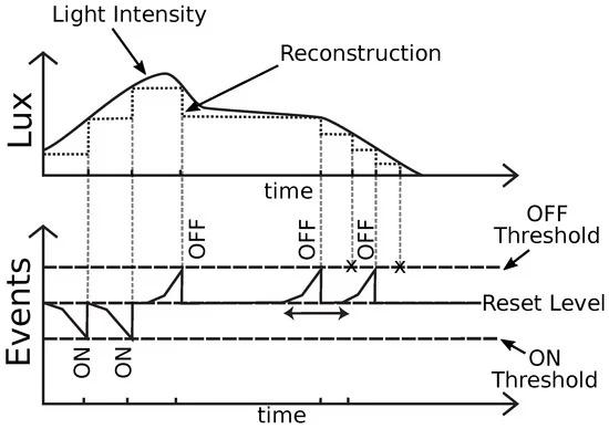
Figure 1. Principle of operation of events cameras [12,22]. As brightness increases until reaching the “on threshold” value, positive events are generated. Conversely, as brightness decreases until reaching the “off threshold”, negative events are triggered. Due to the refractory period, events have a limitation on consecutive spiking, as indicated by an ‘x’.
The main characteristics of the events cameras are the following: the spatial resolution, determined by the number of pixels in the image sensor; the dynamic range (DR), range of brightness levels (difference between brightest and darkest detectable intensities) that the event camera can capture (expressed in dB); the temporal resolution, defined as the discrete measurement resolution of the event, characterized by the time unit of the event timestamp detection time [23]; the maximum throughput, referring to the highest data rate the camera can output to the shared bus, typically in million events per seconds (Meps); the latency or the time delay between the occurrence of an event and the transmission of the data to the output bus; and the contrast sensitivity, which is the sensitivity to changes in brightness that report events.
The following subsections provide the background for the DVS pixel, and the potential impact of the key parameters on optical camera communication systems, bandwidth, the refractory period, and bias sensitivity.
3.1. DVS Pixel
The DVS pixel circuit transforms light intensity values into events through the following five steps. First, the photoreceptor converts received photons into a photocurrent Then, the analog circuitry transduces the photocurrent into a voltage ), which is logarithmically related to the incident light intensity (using a trans-impedance logarithmic converter, TLC). Second, a source follower (SF) buffer isolates the photoreceptor signal from the rest of the circuit. Third, a switched-capacitor differential amplifier (DA) amplifies changes ) between the current signal and the memorized value, corresponding to the intensity sampled after the last event was reported. Up to this point, all the signals involved are analog. Section 4 involves comparing the amplified signal with ON and OFF thresholds. When either threshold is reached, this triggers the generation of either an ON or an OFF event, which is then transmitted externally from the array. When two or more pixels send digital data values to the shared bus simultaneously, an arbiter protocol named the address event representation (AER) protocol interferes to avoid data collision. The AER protocol queues the digital data, which await their turn to be sent by the shared bus. Due to the waiting time, the timestamp corresponds to the moment of data transmission to the output bus and not to the time of event detection (latency effect). When using this arbitration mechanism, the arbiter ensures that a row or column, once serviced, is guaranteed not to be served again until all other rows and columns with registered requests have been completed (non-greeding) [24]. In the last part, once the event is sent out to the shared bus, the AER protocol sends an acknowledgment digital signal to reset the value stored in the DA, memorizing a new intensity value and consequently allowing the pixel to spike another event [12]. The scheme of the DVS pixel can be seen in Figure 2.
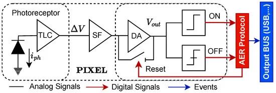
Figure 2. DVS architecture. This diagram illustrates all steps involved in transforming analog light intensities into events. All the pixels share the same AER arbiter and output bus.
3.2. DVS Main Parameters
The bandwidth of the DVS pixel is related to the maximum stimulus frequency that the pixel circuit can respond to. The latter is governed by the physical characteristics of the pixel construction, namely the parasite capacitance added by the photodiode, and transistors among other causes. On the other hand, the bandwidth of DVS cameras is defined as the maximum number of events that can be sent through the output bus simultaneously. In optical communication systems, a noisy environment can reduce the link performance due to the saturation of the output bus with events that do not carry information (noise). Another cause of bus saturation is the use of multiple blinking transmitters. Therefore, event cameras with large throughput values are more suitable in outdoor environments or when multiple transmitters are used.
Moreover, the refractory period is a parameter that limits the maximum firing rate of individual pixels [22], preventing a small group of pixels from monopolizing the entire bus capacity. After a pixel reports an event to the output bus, a reset signal is generated, setting
to a reset state value independent of the input; therefore, no new events can be spiked.
is held in reset state for a time known as the “refractory period”. Consequently, if the light stimulus changes rapidly, a single pixel of the event camera cannot capture high-speed changes, due to the refractory period effect. Therefore, the refractory period limits the maximum speed rate at which the optical communication link can operate. To overcome this limitation, data from multiple pixels could be considered for detecting fast-change incident light sources, as illustrated in Figure 3.
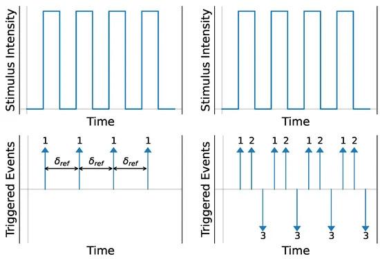
Figure 3. Effect of the refractory period in capturing a high-speed light stimulus. When one pixel (Pixel 1) is considered, it becomes apparent that rapid changes in light intensity cannot be adequately detected. Therefore, it becomes necessary to consider more than one pixel to effectively capture rapid changes. In the example, Pixel 1 and 2 detect the positive brightness changes, while Pixel 3 detects the negative ones.
Finally, event cameras have a programmable bias sensitivity, which adjusts the system’s sensitivity, bandwidth, contrast threshold, and refractory period values [25]. Typically, manufacturers provide the option to configure the bias, but the exact reference value to which each corresponds is not given. This lack of information can be a limitation when trying to model a system accurately. In the DVS camera used for the experiments, five possible values of the bias sensitivity existed: the “VeryLow”, “Low”, “Default”, “High”, and “VeryHigh” that could be set in the camera. Across this range of parameter settings, the camera can detect more (“VeryHigh” sensitivity) or less (“VeryLow” sensitivity) events. Lower bias sensitivity values result in increased noise robustness (defined as non-data-carrying light signals) but require a greater stimulus for the camera to generate events. Conversely, higher values of bias sensitivity enable the camera to detect events with smaller light intensity changes but increase sensitivity to noise. This parameter could be used for adaptive optical communication systems [26], similarly to the automatic gain control loop used in conventional image sensors [22].
4. Fundamentals of n-Pulse Scheme
This section provides both an intuitive description and a mathematical formulation of the n-pulse scheme used for dramatically reducing the complexity of the reception schemes in event-camera-based OCC links.
4.1. Modulation
For transmitting data using an LED, we can employ a modulation technique known as count pulse, where symbols are represented by different numbers of pulses within a symbol period. Each symbol is composed of a specific number of pulses with the same width (τon">
on [s]) and amplitude (A [Lux]). Within a set of symbols, the pulse width is determined by the maximum number of pulses (nmax) and the duty cycle (D) parameter. The duty cycle is defined as the fraction of the sub-period during which the signal is active relative to the total symbol duration. The duration of the pulse, τon">on on, for a given duty cycle (D), the maximum number of pulses (nmax), and symbol time (Ts) is given by Finally, the expression for any symbol, given the prior parameters.
on [s]) and amplitude (A [Lux]). Within a set of symbols, the pulse width is determined by the maximum number of pulses (nmax) and the duty cycle (D) parameter. The duty cycle is defined as the fraction of the sub-period during which the signal is active relative to the total symbol duration. The duration of the pulse, τon">on on, for a given duty cycle (D), the maximum number of pulses (nmax), and symbol time (Ts) is given by Finally, the expression for any symbol, given the prior parameters.
Figure 4 illustrates a modulation example presenting a specific set of symbols. It can be seen that the τg">g
g is different for every symbol, being the largest when the pulse number is minimum (one pulse, s1) and the shortest when the number of pulses is maximum (smax pulses, s4). With this modulation, we can encode up to ⌊ log2(nmax)⌋ bits. For simplicity, we exclude the symbol with no present pulse.
g is different for every symbol, being the largest when the pulse number is minimum (one pulse, s1) and the shortest when the number of pulses is maximum (smax pulses, s4). With this modulation, we can encode up to ⌊ log2(nmax)⌋ bits. For simplicity, we exclude the symbol with no present pulse.
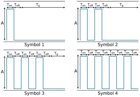
Figure 4. A set of symbols illustrating n-pulse modulations is displayed. The parameters used include a maximum number of pulses (nmax) equal to 4 and a duty cycle (D) equal to 0.5. Each symbol contains a specific number of pulses within the symbol time. With this configuration, we can encode 2 bits per symbol.
4.2. Demodulation
For the use of this particular modulation technique at the transmitter, where each symbol has a different number of pulses, we expect to have a different number of events at the receiver side depending on the transmitted symbol. This is likely due to the response of the DVS camera, which is sensible to brightness changes as explained in Section 3. Therefore, depending on the number of events received, the data would correspond to a specific transmitted symbol. To illustrate the above, in Figure 5, we show the event distribution of positive events at the receiver side for two transmitter frequencies, 10 Hz and 100 Hz, and four different symbols (from 1 to 4 pulses in each symbol period).
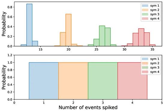
Figure 5. Distribution of the events on the receiver side for different transmitted symbols, and frequencies; 10 Hz (top) and 100 Hz (bottom). In both figures, it can be seen that all symbols are completely separable on the received side.
To construct the event distribution, we repetitively transmit each symbol and, at the receiver, count the occurrences of positive events during each symbol period. Subsequently, we normalize the received event count by the total number of transmitted symbols. We can note that depending on the number of received events, we can decide if the data correspond to a specific symbol. For a frequency of 10 Hz, if the received events are between 12 and 14, the transmitted symbol is likely to be symbol 1. In the same way, if the received events are between 30 and 35 events, the transmitted symbol is likely to be symbol 4. In the example with a transmitter frequency of 100 Hz, the number of pulses at the received side is the same as the transmitted symbol, meaning that if the demodulator counts 1 pulse, the received symbol would be symbol 1, and so on. These meaningful results imply that the candidate demodulator would only need to count the number of events in every period of the symbol time to estimate the transmitted symbol. In practice, counting transitions of events (from positive to negative) yields more accurate results. This straightforward method proves to be effective as long as the distribution of events on the receiver’s side is distinguishable and separable.
As a consequence, when symbols are completely distinguishable in the distribution space at the receiver’s end, the demodulator will confidently classify each set of samples (events received in a symbol period) as one of the possible symbols with high probability enabling effective data demodulation. However, in cases where symbols overlap, the demodulator will classify samples with low probability, resulting in symbol error classification, and degrading the performance of the OCC link. This particular scheme reduces the demodulator complexity and energy consumption, a necessary condition for implementing OCC in real-time or constraint systems.
5. Methodology
In this section, we present a comprehensive overview of the experimental setup used to conduct the experiments, the methodologies employed for implementing data transmission and reception, and the metrics utilized to evaluate the system’s performance.
5.1. Experimental Setup
Figure 6 shows the experimental setup used for testing the OCC link performance considering different parameters. For the transmitter, we used an SMD 1 mm × 0.5 mm LED (20 mA) powered and controlled by a waveform generator. This configuration enabled the LED to blink with configurable light offsets (A) [Lux] and switching frequency (ft) [Hz] values [27]. The purpose of using a small LED was to avoid stimulating a large region at the receiver. This allowed the stimulated pixels to maintain a reset state for a short period, making them capable of detecting high-frequency transmitted data, as explained in Section 3.2.
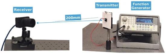
Figure 6. Experimental setup showing an LED as a transmitter controlled by the function generator and an event camera as the receiver. With this configuration, various parameters of both the transmitter and the receiver could be adjusted to conduct experiments with different values representing different scenarios.
To assess the viability of n-pulse modulation, we conducted experiments in a dark room, using a distance of 200 mm. The use of a dark room aimed to prevent the stimulation of other regions by external light sources at the receiver, which could have introduced non-carrying data at the output bus, saturating it and potentially affecting the overall system performance. In addition, the stimulation of a large number of pixels would have increased the negative effects of the refractory period.
For the receiver side, we used a DVXplorer event camera from inivation (Zürich, Switzerland). Its main parameters are depicted in Table 1. A lens with f/1.6 and 4–12 mm focal length was mounted on the camera during the experiments.
5.2. Methods
In this section, we explore the methods employed to establish a viable communication link. Synchronization facilitated the detection of the start frame delimiter, while an additional guard time was implemented to enhance the effectiveness of symbol detection. Finally, we present a detailed description of the procedures used for identifying the transmitter’s pixel location and demodulating symbols.
5.2.1. Synchronization
To synchronize the received data and detect the beginning of the packet, we added a start frame delimiter (SFD) with a duration of three symbol periods.An SFD must differ from any symbol being transmitted, ensuring easy detectability. It comprised two periods of fast transitions and one period of no signal. The particular shape of the SFD, was designed for easy detection at the receiver end. In Figure 7, we show the start frame delimiter at the transmitter and how these data were received at the event camera.
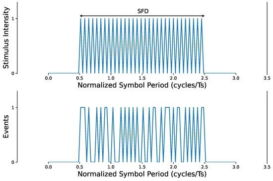
Figure 7. In the upper image, we can observe the start frame delimiter at the transmitter side, while the lower image displays the data captured by the event camera.
It can be noted that, due to various factors, the received signal may not capture all transitions from the transmitted signal. Nonetheless, it deviates sufficiently from the shape of n-pulse symbols, making it distinguishable. For detecting the SFD, the demodulator counts the number of transitions from positive events, followed by negative events throughout 2 symbol periods. If the demodulator registers a count exceeding the potential number of maximum transitions for n-pulse-modulated symbols, it effectively detects the start of a frame.
5.2.2. Extra Guard Time
During the experiments involving the repeated and consecutive transmission of various symbols, the distribution of events at the receiver side became overlapped. This adverse effect could have resulted in a poor performance for the OCC link. Consequently, we introduced an additional extra guard time, comprising one symbol period with no present signal, after every transmitted symbol. The distribution of events with this extra guard time showed an improvement in terms of separability. The symbols constructed with the extra guard time and the use of the start frame delimiter are illustrated in Figure 8.
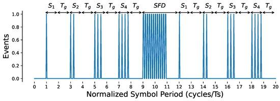
Figure 8. The signal at the transmitter side consisted of four symbols (1, 2, 3, 4) followed by a start frame delimiter and an additional four symbols (1, 2, 3, 4). The inclusion of an extra guard time Tg resulted in improved separability of the signal at the receiver.
5.2.3. Procedures
We tested the experimental setup using the n-pulse modulation scheme with various transmitter and receiver parameters. For the transmitter, we employed different light offsets (Lux), ranging from subtle illumination (13 Lux) to high brightness (75 Lux), ensuring operation within the safe range of the LED’s capabilities. We also tested different frequency values (Hz), which closely aligned with the findings of [19]. For the modulation, we used different values of duty cycle (D) and a maximum number of pulses nmax equal to 4, encoding 2 bits per symbol, as explained in Section 4.1. By selecting these parameters, we tried to strike a balance between the number of modulated bits per symbol and the low cardinality of the symbol set. For the receiver, we used different bias sensitivity values. As explained in Section 3.1, this parameter sets the temporal contrast threshold and the refractory period values. This setting determines the camera’s ability to detect, for instance, subtle luminosity variations or rapid changes in the stimulus generated by the transmitter. We transmitted a random word encoded with ASCII code. Each character was represented by eight bits, and the word length consisted of 50 characters. This transmission was repeated 20 times. In total, we transmitted 8000 bits. For each character, we used a start frame delimiter every 8 bits (4 symbols in this setup) and an additional extra guard time of 1 symbol, as explained in Section 5.2.2.
The system initiated the detection of modulated lights, identifying pixels that exhibited spikes caused by the blinking LED. It constructed a synthetic frame by aggregating all events (both positive and negative) for each pixel. Subsequently, the synthetic frame values were normalized to obtain “intensity” values ranging from 0 to 255. Then, to distinguish the presence of the blinking LED pixels from the rest, an automatic image thresholding technique was applied, namely Otsu’s method [8]. This method segregated pixels into two classes, one that corresponded to pixels stimulated by the LED (high number of events) and the other by different noise sources or not stimulated (low numbers of events) [28]. This method is effective as long as the receiver and transmitter remain stationary.
Then, for the group of pixels stimulated by the light source, the demodulator performed the alignment process for the received event data. It detected the start frame delimiter by counting transitions from positive events followed by negative events throughout 2 symbol periods, as explained in Section 5.2.1. When the count exceeded the potential number of maximum transitions for n-pulse-modulated symbols, detection was achieved. After this, the demodulator performed the symbol decoding process, counting transitions of events for every symbol period (considering the extra guard time used). Finally, the demodulator searched for the next SFD, and the process was repeated.
All operations were coordinated by a computer. Consequently, to conduct the experiments, the computer initially configured the signal waveform generator to set up the LED with specific frequency and amplitude values. Subsequently, data representing the signal were generated and loaded into the signal waveform generator using a script. This script took as input the characters to be encoded and the modulation parameters (maximum number (nmax) and duty cycle (D)). Once all configurations were completed, the computer proceeded to gather events with the camera and sent the start signal to the LED to initiate data transmission for a specific duration (in seconds). The communication system pipeline can be observed in Figure 9.
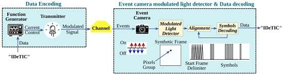
Figure 9. Communication system pipeline, considering the data encoding system and the event camera modulated light detector, in conjunction with the data decoding.
Among the group of pixels obtained by the detection of the modulated lights process, we observed through experiments that the performance of the pixels varied substantially. This difference could be attributed to the fact that the light stimulus did not reach every pixel in the same manner or with the same energy. As in this work we are introducing and testing a new modulation method, the procedure for choosing the right pixel for demodulation was outside the scope of our study.
5.3. Metrics
In this section, we present, define, and describe the evaluation metrics used to assess the system’s performance, including the bit error rate, spectral efficiency, and energy.
5.3.1. Bit Error Rate
For evaluating the optical camera communication link, we employed the bit error rate (BER) metric, computed as the total number of incorrect received-demodulated bits of the total number of bits transmitted. When N bits are transmitted, the minimum BER achievable is BERmin≤1N.">
(5)5.3.2. Spectral Efficiency
The spectral efficiency, a measure of the performance of channel encoding to utilize bandwidth (BW) efficiently, was defined as the average number of bits per unit of time that could be transmitted per unit of bandwidth [bits/s/Hz]. The spectral efficiency (η">) for the particular n-pulse modulation used was approximate as follows:
(6)where Rb is the bit rate, also expressed as /s) and BW is the bandwidth that can be represented as / Therefore, the bandwidth efficiency is given by
(7)5.3.3. Energy
The average energy (E) of the n-pulse modulation set of symbols (S), for a given maximum number of pulses (nmax), in a symbol period (Ts) is given by
E¯S=1nmax∑i=1nmaxP·D·inmax=P·D2·nmax+1nmax,">
(8)where the electrical power (P) can be computed as P=V·I"> It can be observed that the energy is primarily influenced by the duty cycle, rather than the maximum number of pulses.
6. Results and Discussion
The sensitivity and performance of the communication links were analyzed as a function of various parameters. We experimented with different values of pulse width, amplitudes, and bias sensitivity in our experimental setup, evaluating their impact on the bit error rate.
For the tested parameters, which included transmitter frequency [Hz], the maximum number of pulses (nmax), and pulse width for n-pulse modulation, as well as receiver bias sensitivity value, the system achieved error-free reception, at least for a group of pixels. These promising results can be largely attributed to the utilization of a controlled, noise-free environment.
6.1. Bit Error Rate for Different Pulses’ Width
In Table 2, we present the bit error rate results considering various values of the duty cycle (D), defined in Section 4.1. The amplitude, frequency, and bias sensitivity remained constant across all scenarios. Considering the duty cycle, values close to 0.5 yielded better results than those near the extremes. Given that the demodulator counted transitions of events to decode data, as explained in Section 4.2, having duty cycle values close to the extremes made the duration of pulses (τon">on
on) or the duration of the absence of pulses (τoff">off
off) very short, respectively. This short duration made it less likely for the receiver to capture the fast amplitude changes, thus failing to detect the start of a frame or the transmitted symbol itself, ultimately degrading the overall system performance.
Table 2. The bit error rate is presented for different duty cycle (D) values of n-pulse modulation, transmitting 8000 bits. The distance between the transmitter and receiver was 200 cm. The transmitter operated at a frequency of 200 Hz. The maximum number of pulses for n-pulse modulation (nmax) was set to 4. Additionally, the receiver’s bias sensitivity was configured to “default”.
6.2. Bit Error Rate for Different Amplitudes
Considering different values of the transmitter signal amplitude, Table 3 presents the results of the BER for specific experimental setup parameters and the four best-performing pixels. The results are ordered in descending order. It can be observed that for low amplitude values, while some pixels received the data without errors, others performed poorly. This behavior contrasted with the greater amplitude values, where all the pixels performed without error.
Table 3. The bit error rate is presented for different transmitter amplitudes, maintaining a constant distance of 200 cm between the transmitter and receiver. The transmitter operated at a frequency of 200 [Hz]. For the n-pulse modulation, a duty cycle (D) of 0.4 was applied, with the maximum number of pulses (nmax) set to 4. Additionally, the receiver bias sensitivity was configured to “high”.
For low values of the transmitter signal amplitude, it is unlikely that the demodulator could separate events caused by the signal from those caused by the noise. Additionally, considering a given stimulus contrast, the probability that a pixel outputs an event is not spatially and temporally uniform, resulting in varied performances of the pixels [29]. Finally, the use of higher amplitudes generates a sufficient contrast threshold difference required to trigger events, effectively stimulating a greater portion of the pixels.
6.3. Bit Error Rate for Different Bias Sensitivity
Table 4 presents the BER results for the different bias sensitivity values and the 12 best-performing pixels. As discussed in Section 3.2, the bias sensitivity set the refractory period and threshold contrast sensitivity, influencing the capabilities of the OCC link. For the “default” bias sensitivity value, 4 pixels received data without errors, while for the “High” and “VeryHigh” values, 8 and 12 pixels showed an error-free reception, respectively. The performance of the subsequent pixels degraded rapidly. This indicates that higher bias sensitivity values for the receiver enhanced the OCC link performance, due to smaller values of the refractory period and threshold sensitivity. This configuration allowed the receiver to capture more events than when using smaller values; therefore, in a controlled and non-noisy environment (in the absence of external light sources, or movement), it yielded better results. The same behavior occurred for the other experimental setup parameters.
Table 4. The bit error rate was evaluated for various receiver bias sensitivity values, with a distance of 200 cm between the transmitter and receiver. The transmitter operated at a frequency of 100 Hz and a light stimulus irradiance of 13 Lux. For the n-pulse modulation, a duty cycle (D) of 0.4 was applied, with a maximum number of pulses (nmax) set to 4.
In Table 5, we present the total number of events gathered for the different values of bias sensitivity. Higher values resulted in capturing more events, with a similar trend observed for the central duty cycle values. While these findings might imply that OCC systems benefit from increased bias sensitivity, there are significant drawbacks in real-world scenarios. The presence of noise from external light sources or movement can rapidly increase the number of events captured by the receiver. Consequently, the bus output may saturate, as detailed in Section 5.1, introducing undesirable delays and struggling to manage all pixel requests. This, in turn, could exacerbate the negative effects of the refractory period, degrading the overall system performance.
Table 5. Total number of events for different receiver bias sensitivity values. The distance between the transmitter and receiver was 200 cm. The transmitter operated at a frequency of 200 Hz. The maximum number of pulses for n-pulse modulation (nmax) was set to 4.
The abovementioned issue, which may appear as a problem, can also be viewed as an opportunity. Within the new paradigm of joint sensing and communication (JC&S), the receiver can dynamically adjust the bias sensitivity value based on the number of events gathered (sensing) to enhance the performance of the OCC link (communication). In noisy environments, where the number of events increases rapidly, the receiver could set lower bias sensitivity values or higher values in low-noise environments, to improve OCC link performance.
6.4. Comparison with Other Approaches
As discussed in Section 2, studies on implementing OCC systems with event cameras as receivers often rely on computationally expensive algorithms, whether for locating transmitters or demodulating data, while also exhibiting scalability or replicability limitations. In [18], the algorithm for detecting pixels potentially associated with modulated light sources employed a subsampling technique that was linearly dependent on factors such as image size (height, width) and transmitter frequency, leading to scalability challenges. Additionally, the system’s performance was influenced by the size of the pixel cluster within the synthetic frame, imposing limitations based on the transmitter dimensions or the distance between the transmitter and receiver. Furthermore, in [19], the detection of LED transmitter pixels involved computationally intensive algorithms such as image morphology and blob tracking in a sliding window, which imposed restrictions on the hardware implementation. Additionally, the demodulation technique relied on numerous heuristic parameters, making it challenging to implement across various scenarios, hindering its applicability. In contrast, our work focused on a different approach: the detection of modulated lights was performed using an automatic image thresholding technique. Furthermore, the demodulator detected event transitions for both synchronization and decoding by using a pulse count-based classification, making this a highly efficient method capable of being implemented on any hardware platform.
In terms of spectral efficiency, D=0.5">=0.5
=0.5 was the best-case configuration.However, as M increased, the energy efficiency of our scheme tended to equal OOK. Despite the slight penalty on the frequency domain, the advantage achieved in terms of complexity reduction on the receiver side made the adopted family of modulation schemes preferable in most cases. As was aforementioned in Section 1, neuromorphic cameras can provide JC&S (and positioning) capabilities at no additional cost, which could enable their use within the 6G paradigm as a support subsystem for other high-speed technologies such as mmWave, LiFi, and probably the successors of 5G New Radio. In general terms, the signaling, sensing, and positioning-related data streams will require sufficiently small bandwidths so as to consider N-pulse modulation for performing data transmission, with a power budget very similar to OOK and with a dramatically lower complexity at the receiver, which ultimately would impact on the hardware requirements for signal processing and therefore on the power budget of the receiver.
7. Conclusions
In this work, the implementation and evaluation of an OCC link using an LED as transmitter and event camera as receiver was presented. The data were encoded using n-pulse modulation, enabling the reception of separable symbols at the receiver end. As a result, the demodulation process becomes highly effective and computationally efficient, requiring the demodulator to count transitions of events for symbol demodulation. Through this approach, we demonstrated error-free data reception in specific scenarios.
We tested the n-pulse modulation scheme, in terms of bit error rate, using various parameters, including the amplitude and frequency of the transmitter, different n-pulse modulation configurations, and diverse bias sensitivity values for the receiver. When considering the width of pulses in n-pulse modulation, the system performed better with duty cycle values close to 0.5. Extreme values resulted in short pulses and brief pulse absences, hindering the demodulator’s ability to capture rapid amplitude changes, and consequently degrading the overall system performance. In the results obtained with different amplitudes, the system exhibited improved performance at higher values. Higher amplitudes generated a significant contrast threshold difference, which is necessary to trigger events, effectively stimulating a larger portion of pixels receiving correctly transmitted data. In terms of bias sensitivity, higher values enhanced OCC link performance in terms of BER. Setting higher bias sensitivity values resulted in a reduced refractory period and threshold sensitivity, enabling the receiver to capture more events and yielding better results.
All experiments were conducted in a dark room at a distance of 200 mm, mitigating the influence of external light sources on other receiver regions. This prevented potential saturation of the output bus, preserving the overall system performance and ensuring that the automatic method for detecting the region of interest (ROI) worked as expected. However, the negative effects of the refractory period at the receiver are exacerbated when using a high transmitter frequency, employing short distances between the transmitter and receiver, or when the transmitter LED has large dimensions, degrading the system’s performance. Furthermore, when computing the bit error rate, we specifically chose the best-performing pixels. However, the selection criteria for demodulation pixels were beyond the scope of this study, as our focus was on demonstrating the feasibility of the proposed communication scheme.
These results suggest that the receiver could dynamically optimize the bias sensitivity value based on the gathered events, to enhance OCC link performance. In noisy environments with a rapid increase in received events, the receiver may set lower bias sensitivity values, whereas, in low-noise environments, higher values could be applied to improve OCC link performance. This kind of configuration is framed within the new paradigm of joint sensing and communication (JC&S).
The results presented in this paper, focusing on optical camera communication links using n-pulse modulation, can serve as a foundation for future experiments. It will be crucial to explore various scenarios, including longer distances between the transmitter and receiver or outdoor environments, to further assess the capabilities of this modulation.