Abstract
This work experimentally investigated the wake-up behaviors of hafnium oxide-based ferroelectric capacitors by manipulating the interval time between each characterization cycle. Both Positive-Up–Negative-Down (PUND) and Negative-Down–Positive-Up (NDPU) waveforms were used as the stress and measurement waveforms in the experiments. It was found that the imprint occurs as the total interval time increases to a several-seconds level. However, this only affects the remnant polarization (PR) of ferroelectric capacitors when stressed by NDPU waveforms, since the voltage amplitude saturates under the PUND stress conditions and does not influence the PR. The wake-up behavior has been proved to be caused by the defects redistribution during electrical cycling. Notably, when using PUND waveforms, the change in the interval time can result in different increase rates of PR, indicating the possibility of recovery during the intervals. This recovery leads to a slower wake-up when cycling with a longer interval time. Moreover, it is observed that this PR recovery could reach saturation after several seconds of the interval time. This comprehensive investigation of wake-up and imprint behaviors can provide new insights to evaluate and enhance the reliability of ferroelectric memories.
Keywords: ferroelectric; wake-up; imprint
1. Introduction
In recent years, with the development of neural networks, research in Artificial Intelligence (AI) has experienced explosive growth. However, at the hardware level, the increasing demand for memory capacity and bandwidth makes it challenging to meet the growing needs. In order to overcome the limitations of the memory wall, both academia and industry have begun to focus on the research of emerging memories. The conditions required for the commercialization of emerging memory include integrability with core devices, high read/write speeds, scalability, low power consumption, and good reliability. Within the study of emerging memories, HfO2-based ferroelectric (FE) oxides have been extensively investigated owing to their non-volatile property, CMOS compatibility, and dimensional scalability [1,2]. Moreover, traditional ferroelectric materials such as lead zirconium titanate (PZT) or strontium bismuth tantalite (SBT) have a very low band gap and coercive field, which makes them easy to breakdown and lose the storage state. Compared with traditional ferroelectric materials, the HfO2-based FE material has a higher band gap (5.6 eV) which enhances the breakdown voltage. Additionally, it has a higher coercive field and results in a longer retention time. This makes it more suitable for ferroelectric random access memory (FeRAM) applications [3]. Owing to the potential application of the HfO2-based FE oxides, the original article on the ferroelectric properties of HfO2 has been cited over 1500 times since the first proposal of HfO2-based FE oxides in 2011.
However, there are still reliability concerns regarding HfO2-based FE memory applications. On one hand, to determine the polarization direction of a ferroelectric devices, it is typically necessary to attempt switching its polarization direction, meaning that the read operation of ferroelectric devices is destructive. For ferroelectric devices, repetitive operations can lead to device fatigue, thus requiring sufficient endurance. On the other hand, unlike ideal devices, real devices exhibit a depolarization field on the ferroelectric layer, which reduces the retention time of ferroelectric memories. Moreover, there are some reliability concerns related to unstable polarizations, behaving as the wake-up and imprint effect [4,5,6,7,8]. The wake-up refers to an increase in remnant polarization (PR) during an endurance test. And the imprint manifests as the horizontal shift of both the coercive field (Ec) and hysteresis loop, which usually occurs during a retention test [9,10]. These unsolved problems pose challenges to HfO2-based FE memories for reliable operation and long-term stability.
In previous reports, several possible mechanisms have been proposed to explain the wake-up behaviors observed in ferroelectric films. One of these mechanisms suggests that defects within the film can migrate from the FE layer and electrode interface towards the middle of the film during the wake-up, reducing the local built-in electric field generated by charged defects [11,12]. As the ferroelectric originates from the polar orthorhombic phase, another proposed mechanism involves a phase transition from the tetragonal phase to the polar orthorhombic phase, which is believed to contribute to the wake-up behavior [13].
For the mechanism of imprint behaviors, the imprint effect in ferroelectric (FE) devices is closely related to the charge trapping caused by the depolarization field. In an ideal FE capacitor, the polarization can be completely screened by charges present in the electrodes. However, in real devices, the polarization is not fully screened due to the presence of an interface layer [14]. This incomplete screening results in the formation of a depolarization field across the FE layer, which further enhances the phenomenon of charge trapping [15]. These injected charges establish an additional electric field, causing the voltage shift of the P–V curves and manifesting as the “imprint” phenomenon.
In non-volatile memory circuit applications, not only one single degradation behavior occurs to the memory device during its operation. For FE capacitors, the wake-up and imprint effects can occur simultaneously during various operational states, including program, erase, and idle states. The idle state here means the duration at 0 V bias (i.e., the interval time during each cycle). It has already been explained that the wake-up effect is associated with defect redistribution driven by the electric field [12]. The duration of idle state (0 V bias) may influence wake-up behaviors owing to the existence of a depolarization field [16]. Additionally, retention loss and imprint could also occur during the idle state and potentially impact polarization behaviors [10]. Consequently, there is a critical need to study the wake-up and imprint issues with different interval times, which has not been sufficiently studied yet.
In this work, a comprehensive investigation was conducted to understand the wake-up and imprint behavior of ferroelectric (FE) capacitors by varying the interval time between each cycle of polarization characterization. During the measurement of HfO2-based FE memories, both the wake-up and imprint phenomena simultaneously occur. Although the imprint effect may lead to changes in PR, it is important to note that when the measurement voltage amplitude reaches saturation, the imprint effect might not be reflected in the remnant polarization. The experimental data clearly demonstrate that the wake-up phenomenon is related to the redistribution of defects within the FE material. Furthermore, it was observed that a relaxation behavior occurs during the interval time excluding the effect of imprint, which could reach a saturation point within a few seconds. These findings provide important insights into the fundamental mechanisms of wake-up and imprint in FE capacitors.
2. Device Processing and Characterization Method
In this study, HfO2-based FE capacitors were used with the structure of W/TiN/Hf0.5Zr0.5O2/TiN. The bottom electrode (BE) of 15 nm TiN layer was deposited by ALD at 400 °C on a pre-clean heavily doped Si substrate, using TiCl4 and NH3 as the precursors. Then, the FE film of 10 nm Hf0.5Zr0.5O2 layer was deposited by ALD at 270 °C. The precursors used during the deposition were TEMAH and TEMAZ for the Hf and Zr sources, respectively. Plasma O was employed as the oxygen precursor. Following that, a top electrode (TE) was formed with 15 nm ALD TiN and 100 nm sputtered W. Then, the crystallization anneal was performed at 500 °C, lasting 60 s.
The waveform pattern for this study is schematically illustrated in Figure 1a. Both the Positive-Up–Negative-Down (PUND) and Negative-Down–Positive-Up (NDPU) waveforms were used as the stress and measurement waveforms to study the impact of the interval time (Tinterval) on FE degradations. To ensure an accurate evaluation of the real performance and eliminate the impact of retention loss, each polarization characterization cycle consists of two continuous periods. The data analyzed in this study are extracted from the second period. Notably, each cycle for polarization characterization was separated by the Tinterval. To investigate the influence of a Tinterval of 0 V bias on the wake-up effect and imprint behavior, the duration of the Tinterval can be adjusted within a wide range, from nanoseconds to a few seconds.

Figure 1. (a) The adopted waveform for PR characterization and interval time study. (b) Diagram of the experimental setup for this study. The input impedance was configured to 1M Ω and the output impedance was set to 50 Ω. The device voltage is tracked by measuring the difference between two channels, and the corresponding current can be calculated as Vo/50.
In Figure 1b, the stress and measurement processes were conducted using the F3000 equipment from Zhejiang Liryder Technology Co., Ltd. (Hangzhou, China). The waveforms were generated by the Ch1 of the equipment. And this Ch1 is connected to the back electrode (BE) of FE capacitors, and the signal generated is recorded as Vi. The response voltage from the top electrode (TE) of the FE capacitors is measured by the Ch2 and recorded as Vo. To ensure proper signal integrity and impedance matching for high-speed measurements, the output impedance of the Ch1 connected to BE was set to 1 MΩ to eliminate the signal reflection, since the device under test (DUT) also has high impedance. On the other hand, the Ch2 connected to TE has an impedance of 50 Ω. It is important to note that the voltage across the device is the variance between Vi and Vo, representing the voltage across the FE capacitors. The device current can be calculated by dividing Vo by the 50 Ω impedance.
When conducting measurements with Tinterval values less than 1 ms, all the data were captured from the same screen. This means that the results for each cycle were recorded continuously and appeared together. However, when dealing with Tinterval values in the milliseconds scale the data for each cycle were captured separately, which is limited by the available data length. Instead of being displayed continuously, the data for each cycle were stored or analyzed individually. This approach allows for a more detailed examination of the behavior and characteristics of the FE capacitors at a longer Tinterval.
3. Results
The test results with both PUND and NDPU waveforms are plotted below. For the devices stressed with PUND waveforms, Figure 2a shows the increase in double remnant polarization (2PR) with applied cycles. The increasing rate decreased with a longer Tinterval, which is saturated for 3.5 s and 10 s Tintervals. As shown in Figure 2b, the 2PR increases, and the coercive voltage (Ec) does not show an obvious shift with a 100 ns Tinterval. However, as the 10 s Tinterval results shown in Figure 2c, in addition to the increase in PR, the FE hysteresis loop, there is a Ec shift to the positive direction, which is called “imprint” [17]. Therefore, it can be concluded that wake-up and imprint occur simultaneously during the measurement with a long Tinterval.
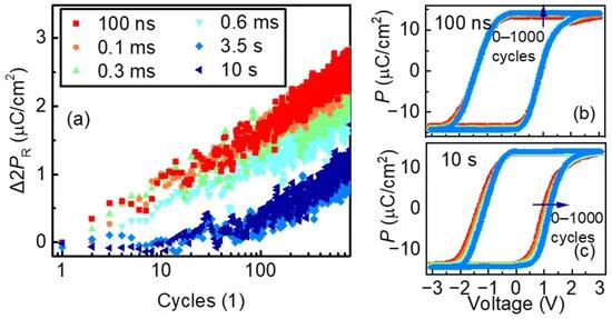
Figure 2. FE capacitors are stressed with PUND waveforms. (a) The change in double remnant polarization Δ2PR varied with applied pulses cycles with different Tintervals, ranging from 100 ns to 30 s. (b) The change in P–V curves during cycling of the 100 ns Tinterval shows few Ec shift. (c) Another cluster of P–V curves shows an obvious positive Ec shift under the cycling of a long Tinterval of 10 s.
Furthermore, the devices subjected to NDPU stress waveforms have been evaluated, and the test results are presented in Figure 3. In Figure 3a, it could be observed that the increase rate of PR also decrease with the longer Tinterval. However, unlike the results in Figure 2a, the change in double remnant polarization (Δ2PR) decreases with the applied cycles, and the curves are not the same for Tinterval values of 3.5 s and 10 s. The P–V curves in Figure 3b are similar to Figure 2b. Figure 3c shows P–V curves shift to the negative direction and PR decrease. The reason behind this phenomenon will be explained in further detail later in this study.
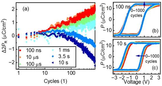
Figure 3. FE capacitors are stressed with NDPU waveforms. (a) The change in double remnant polarization Δ2PR varied with the applied pulses cycles. (b) The change in P–V curves during cycling of the 100 ns Tinterval and (c) a 10 s Tinterval.
3.1. Imprint Caused by Depolarization Filed
The imprint behavior is discussed in this section. Regarding the imprint effect, it is observed that the voltage shift occurs with a long Tinterval in Figure 2c and Figure 3c. The imprint phenomenon has been extensively discussed and is known to be associated with the depolarization field (Ed), which plays a significant role in retention loss and imprint effects. The Ed is caused by the imperfect compensation of the polarization. When the applied voltage is reduced to 0 V after subjecting the devices to PUND waveforms, the equivalent circuit is illustrated in Figure 4. The switching layer and the non-switching layer are connected in series.
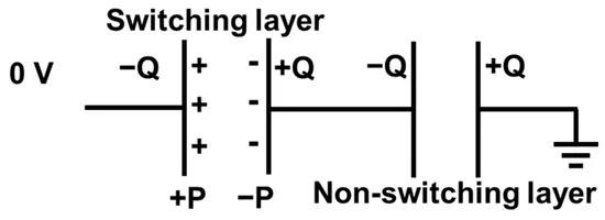
Figure 4. The equivalent circuit at 0 V bias after PUND waveform shows the switching layer and the non-switching layer are connected in series.
Due to the non-volatile nature of the device, the stored charges in the switching (FE) layer can generate an electric field on the non-ferroelectric layer, and then induce an electric field on the non-switching layer. This will result in the depolarization field (Ed) within the FE layer as the total applied voltage is 0 V, [18], as described in (1). Here, the saved charge (Q) corresponds to the measured remnant polarization (PR), which may not be the same as the true polarization of the switching layer (P). The capacitance of the non-switching layer is represented by CI, and dF represents the thickness of the FE film. In addition, the electric field on the non-switching layer (EI) can be expressed by (2). In this equation, εI represents the dielectric constant of the non-switching layer, and ε0 represents the vacuum dielectric constant. For general cases with a typical remnant polarization (2PR) value of 20 µC/cm2 and εI = 30, the calculated EI would be 7.5 MV/cm. This high electric field can result in charge injection across the non-switching layer and stored in the interfacial layer. The injected charges across the non-switching layer can contribute to the observed voltage shift.
To investigate the imprint behavior numerically, the biased voltage of the device is defined as the Ebias and is calculated by (3), where Ec+ and Ec− represent the electric field at the zero polarization point on the positive and negative half axis, respectively. Since the imprint phenomenon is induced by the charge injection [19], the time-dependent voltage shift (∆Ebias) can be calculated by (2), where E0 and τ0 are constants [20]. The linear relationship of ∆Ebias and log10t, as shown in Figure 5, demonstrates a linear trend that aligns with (4). However, polarization degradation does not follow this function, and polarization degradation is cycle dependent, instead of time dependent, as shown in Figure 2a. It can be inferred that the response PR for PUND stress is not induced by imprint.

Figure 5. The change in the Ebias with the increased time for PUND stress, the Ebias is time dependent.
Compared with the PUND stress, the results of NDPU stress are plotted in Figure 6. The changes in both Δ2PR the Ebias with the total interval time are time dependent, as depicted in Figure 6a, Figure 6b, respectively. The results indicate that the 2PR decrease is caused by imprint when the interval time exceeds 3.5 s.

Figure 6. The change in the (a) Δ2PR and (b) Ebias with the total interval time for NDPU stress, both the Δ2PR and Ebias are time dependent.
When the PUND waveforms are applied on the device, the PR change is not caused by the imprint while imprint does occur, unlike with the NDPU waveforms. Previous studies [10,21] have reported that imprint behaviors can cause changes in PR. However, it has been observed that when the amplitude of the applied voltage is sufficiently high, the PR does not change with the imprint [22]. In Figure 7a, hysteresis curves with different voltage ranges are shown. And the extracted 2PR are shown in Figure 7b. It is evident from the figure that the 2PR does not increase when the applied electric field exceeds 3 MV/cm. For the PUND stress, the hysteresis curves shift to the positive direction, which means a higher writing electric field than that of the initial state, since the initial Ebias is negative. This suggests that the imprint does not significantly affect the 2PR with the PUND stress when the Tinterval increases to several seconds. In contrast, under NDPU stress, the hysteresis curves exhibit a shift towards the negative direction, resulting in a reduction in the electric field amplitude. This implies that imprint plays a dominant role in the 2PR changes observed during NDPU stress when the Tinterval lasts several seconds. On the other hand, the slower wake-up phenomenon with a longer Tinterval during PUND stress is caused by another mechanism.
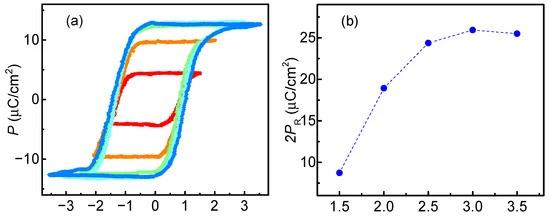
Figure 7. (a) P–E loops with different writing voltage ranges. The curves with different colors represent the measurement with varying voltage magnitudes. (b) The 2PR is a function of the electric fields; the 2PR keeps increasing and is saturated above 3 MV/cm.
3.2. Wake-Up Mechanism Analysis
In this section, several hypotheses are proposed and discussed. Some theories could explain the wake-up behavior. Firstly, the charged defects moving from the FE/electrode interface to the middle of the FE layer could reduce the built-in electric field and enhance PR. Another possible explanation is that the wake-up effect observed during voltage cycling could be caused by the degradation of the non-ferroelectric layer at the interface. This degradation could result in an increase in leakage current, resulting in a reduced depolarization field across the switching layer [23,24]. Consequently, this lower depolarization field serves as a trigger for the wake-up effect. Another possible cause of the wake-up effect could be the transformation of the non-switching layer from a t-phase to an o-phase, resulting in its conversion into a switching layer. And some studies have suggested that wake-up behavior can be induced by phase changes [13,25] because the relative dielectric constant (εr) of o-phase and t-phase is 25–30 and 35–40, respectively [25], the phase change can be observed through variations in the εr since different phases exhibit different εr values. Furthermore, the degradation of the non-switching layer can lead to an increase in the equivalent capacitance of the system, which can also be manifested through changes in the relative dielectric constant εr.
To study the mechanism of wake-up effect, the εr values were examined and obtained from I–V curves for both 100 ns and 10 s Tintervals, as presented in Figure 8a,b. The calculation of εr utilizes the displacement current at high voltage, where the polarization current can be neglected. Equation (5) is used to determine the value of εr, where I is the displacement current, d is the thickness of the oxide layer, S stands for the area of the device, ε0 is the vacuum dielectric constant, V represents the applied voltage, and t is the time.
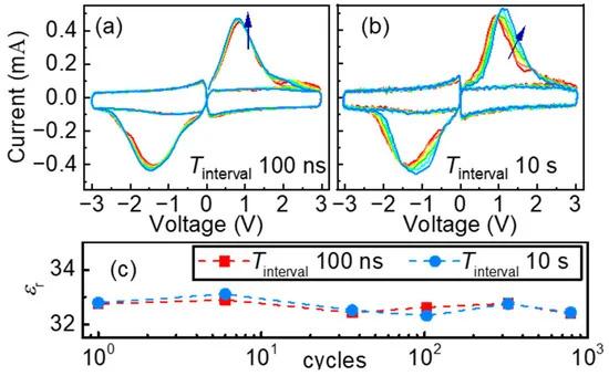
Figure 8. (a) I–V curve varies with the increasing applied cycles (the gradient color from red to blue represent the cycles from 0 to 1000 times) with a 100 ns Tinterval and (b) a 10 s Tinterval. (c) The εr is a function of the applied cycles; the εr is approximately 32.5 and does not show obvious change with the cycles.
The obtained results indicate that the εr of the oxide film is approximately 32.5, which aligns with findings reported in [25,26]. Furthermore, as depicted in Figure 8c, the εr value does not change significantly with applied cycles. This suggests that there is no phase change during the wake-up process. Moreover, these findings suggest that the wake-up phenomenon is not caused by non-switching layer degradation as this degradation would also cause a capacitance change. In conclusion, excluding the two explanations, the wake-up behavior might be caused by the defect migration driven by electric field.
As reported in [27], the oxygen vacancy concentration is highest at the Hf0.5Zr0.5O2/TiN interface, and it decreases with the depth along the FE layer. This distribution of oxygen vacancies generates a local electric field. Based on this observation, the results in Figure 8a show that the local switching current at high positive voltage shifts to the low positive voltage direction, indicating the wake-up is driven by the defects redistribution during electric cycling.
4. Discussion
Based on the above test results, several conclusions can be inferred. Firstly, the imprint could cause a change in the 2PR. However, it is important to note that the 2PR becomes saturated when the applied voltage amplitude exceeds 3 V. This saturation indicates that further increasing the voltage does not significantly affect the 2PR. Secondly, imprint primarily influences the 2PR during NDPU waveforms. In these waveforms, the imprint phenomenon has a noticeable impact on the 2PR values. However, during PUND waveforms, imprint does not induce any significant change in the 2PR. It suggests that the variations in the 2PR observed during PUND measurements are not primarily influenced by imprint effects. Instead, the slower increase in 2PR with longer interval times during PUND waveforms is assumed to be associated with the wake-up relaxation phenomenon.
As reported in previous studies, the wake-up phenomenon can be explained by the migration of charged defects away from the ferroelectric/metal interface [11,12]. In Figure 8a, the I–V curves show that the switching current at high positive voltage decreases while the current at low positive voltage increases. This indicates that the wake-up behavior is associated with the shift of the local internal field (Ebuilt-in). Positively charged oxygen vacancies (Vo) establish a local Ebuilt-in, which leads to a higher switching voltage and a higher back-switching current. During cycling, these oxygen vacancies gradually migrate towards the middle of the ferroelectric (FE) layer, reducing the local Ebuilt-in and resulting in a higher PR. This procedure is illustrated in Figure 9a. Meanwhile, as mentioned earlier, an electric field (Ed) exists at 0 V voltage, which can also impact the positive oxygen vacancies in the hafnium zirconium oxide layer. As shown in Figure 9b, during the Tinterval, Ed can drive the oxygen vacancies back towards the interface, enhancing the Ebuilt-in, and ultimately slowing down the wake-up process. Within a few seconds of the Tinterval, the wake-up rate reaches a saturation point, which may be a result of a balanced electric field.
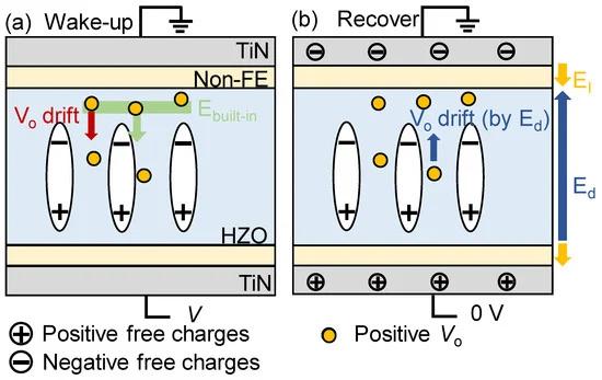
Figure 9. (a) Schematic diagram of the wake-up behavior; the local positive oxygen vacancies (Vo) could build an internal bias. When the Vo migrate to the middle of the FE layer, the internal bias decrease and result in the wake-up. (b) During the Tinterval, the Ed could drive the Vo back towards the interface, and cause a slower wake-up.
5. Conclusions
In this study, the wake-up behaviors have been studied using PUND and NDPU waveforms with different Tintervals ranging from 100 ns to 10 s. Under NDPU stress patterns, the imprint phenomenon occurs during the Tinterval, and it can result in a PR loss when the Tinterval lasts for several seconds. As for the case of PUND stress, by applying a read voltage that achieves polarization saturation, the influence of imprint can be excluded. Experimental results show that the wake-up rate decreases as the Tinterval between each PUND period increases. This wake-up behavior has been illustrated by the defects redistribution from the interface TiN/FE towards the middle of the oxide layer. The relaxation phenomenon is explained by considering the depolarization field driving positive-charged oxygen vacancies back towards the interface. Furthermore, it has been found that the relaxation of the wake-up behavior could be saturated in several seconds. The results of this study could be very helpful for understanding the reliability behaviors of hafnium oxide-based ferroelectric capacitors.