Abstract
The 1.2 kV SiC MOSFET with a buried oxide was verified to be effective in improving switching characteristics. It is crucial to reduce the gate–drain charge (QGD) of devices to minimize switching loss (Etotal). The SiC MOSFET with a split gate and device with a buffered oxide have been proposed by previous studies to reduce the QGD of the devices. However, both devices have a common issue of the concentration of the electric field at the gate oxide. In this paper, we propose the 1.2 kV SiC MOSFET with a buried oxide to reduce the QGD and suppress the electric field crowding effect at the gate oxide. We analyzed the specific on-resistance (Ron,sp), QGD and the maximum electric field at the gate oxide in the off state (Eox,max) according to the width (WBO) and thickness of the buried oxides (TBO). The device with the buried oxide, under optimal conditions, showed lower Eox,max and Etotal without significant increase in Ron,sp in comparison to the device with a conventional structure. These results indicate that the buried oxide can improve the switching characteristics of 1.2 kV SiC MOSFETs.
Keywords: SiC; MOSFET; gate charge; electric field crowding effect; switching characteristics
1. Introduction
Silicon carbide (SiC) power semiconductors exhibit superior performance compared to silicon (Si) power semiconductors owing to their wide bandgap energy, high critical electric field and thermal conductivity [1,2,3,4,5]. SiC devices with wide bandgap energy demonstrate reliable operation even at elevated temperatures due to their lower intrinsic carrier density [1,2]. The high critical electric field of SiC enables the design of a thinner N-drift layer with higher doping concentration compared to Si devices operating at the same rated voltage. The resistance of the N-drift layer accounts for the majority of the total resistance, so SiC devices with thin and high-doped N-drift layer exhibit lower on-resistance and conduction loss. Additionally, SiC devices have high thermal conductivity, ensuring stable performance even at high temperatures [3,4].
SiC devices such as SiC Schottky barrier diodes (SBDs) and SiC metal oxide semiconductor field effect transistors (MOSFETs) are widely used in the rated voltage range from 600 V to over 3.3 kV due to their superior breakdown characteristics and low resistance. Particularly, 1.2 kV SiC MOSFETs are extensively utilized as switching components in electric vehicle on-board chargers, inverters and DC–DC converters [4,5]. However, the gate charge of 1.2 kV SiC MOSFETs are required to be minimized because a large portion of the energy loss occurs during the switching operation of the devices. The gate–drain charge (QGD) is a main parameter that influences the switching characteristics of SiC MOSFETs. High voltage and current are applied simultaneously to the devices when the gate–drain capacitance (CGD) is being charged [5,6]. Several studies to improve the switching characteristics of SiC MOSFETs by reducing the QGD have been reported [7,8,9,10,11,12,13,14,15,16,17].
Baliga’s research group reported the use of a 1.2 kV SiC MOSFET with a split gate to reduce QGD of the device. The split gate has a split structure of a poly-Si gate over the JFET region. The device with the split gate is effective for reducing QGD because the area overlapped between the gate and the drain is reduced [8,9,10,11,12]. However, the device with the split gate presents the issue that the electric field is concentrated at the gate oxide [8,9]. In subsequent studies, they added a p-type layer of high concentration to the bottom of the p-base region to suppress the electric field crowding effect at the device. This p-type layer of high concentration serves to protect the gate oxide by widening the depletion layer in the p-base junction [10,11,12].
Buffered oxide is another structure that can reduce the QGD of SiC MOSFETs. The buffer oxide has the structure where a thick oxide is deposited over the JFET region. The 1.2 kV SiC MOSFET with buffered oxide has lower QGD compared to the device with a conventional structure due to a decrease in CGD [13,14]. However, the protruding shape of the poly-Si gate leads to the concentration of the electric field at the corners of the buffered oxide. The 1.2 kV SiC MOSFET with a tapered buffer oxide has been introduced to address the issue of electric field crowding effect in the device with the buffered oxide [14]. The tapered buffer oxide is characterized by the addition of an angle to the buffered oxide. The device with tapered buffer oxide has shown the ability to disperse the concentration of the electric field at the corners of the gate oxide [7,14].
The device with the split gate and the p-type layer with high concentration needs an additional step for ion implantation [10,11,12,15]. In the case of the device with the tapered buffer oxide, the maximum electric field at the gate oxide in the off state (Eox,max) of the device is highly dependent on the angle of the tapered buffer oxide [14]. Several studies that have investigating the gate reliability of SiC MOSFETs using an analysis of time dependent dielectric breakdown have reported that SiC MOSFETs have reliable electrical characteristics when the Eox,max has been designed below 3 MV/cm [16,17,18]. Therefore, it is necessary to develop the devices for low Eox,max as well as for low QGD.
In this paper, the 1.2 kV SiC MOSFET with buried oxide which has improved switching and electric field characteristics is proposed. We used TCAD simulations to verify the performance of the 1.2 kV SiC MOSFET with the buried oxide. The device with the buried oxide, shown in Figure 1b, has a structure in which the JFET region is etched and filled with oxide. We analyzed the specific on-resistance (Ron,sp), QGD and Eox,max of the devices with the buried oxides according to the width (WBO) and thickness of the buried oxide (TBO) to obtain optimal conditions for the buried oxide. In addition, the switching characteristics of the device with the conventional structure and the device with the buried oxide under optimal conditions were compared. The results showed that buried oxide is effective in improving the switching characteristics of 1.2 kV SiC MOSFETs without deteriorating other electrical characteristics.
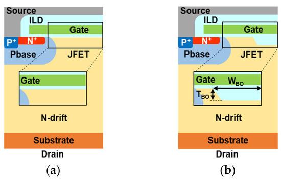
Figure 1. Cross-sectional views of 1.2 kV SiC MOSFETs. (a) The device with the conventional structure and (b) the device with the buried oxide.
2. Methods of Simulations
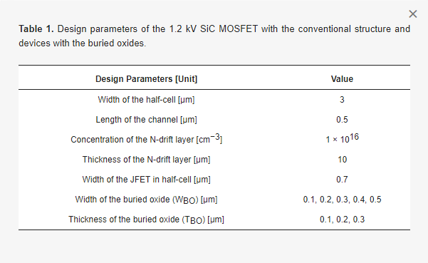
Sentaurus TCAD simulations were used to evaluate the performance of the 1.2 kV SiC MOSFET with buried oxide. For comparison, the 1.2 kV SiC MOSFET with the conventional structure and the 1.2 kV SiC MOSFETs with buried oxides were designed. The simulations were conducted based on the size of a half-cell. The target values for breakdown voltage (BV) and Ron,sp were set at 1560 V and 5 mΩ·cm2, respectively. The cell pitch, channel length, width of the JFET, concentration and thickness of the N-drift layer were designed considering the target BV and Ron,sp [19,20,21]. The width of the JFET from the surface of the N-drift layer, based on the half-cell, is 0.7 μm. The aluminum (Al) concentration of the p-base is highest at a distance of 0.4 μm from the surface of the N-drift layer. At this location of the highest Al concentration in the p-base, the width of the JFET, based on the half-cell, is 0.5 μm. To ensure that the buried oxide does not completely block the JFET region, the WBO was designed to be between 0.1 and 0.5 μm and TBO was designed to be between 0.1 and 0.3 μm. Design parameters of the device with the conventional structure and the device with the buried oxide are summarized in Table 1. To optimize the design conditions for buried oxide, we compared the Ron,sp, QGD and Eox,max of the devices with buried oxides according to the WBO and TBO. The switching loss (Etotal) of the device with the conventional structure and that with the buried oxide under optimal conditions were then compared, revealing that buried oxide is effective in improving the switching characteristics of 1.2 kV SiC MOSFETs.
Table 1. Design parameters of the 1.2 kV SiC MOSFET with the conventional structure and devices with the buried oxides.
3. Results and Discussion
Figure 2 is the Ron,sp of the device with the conventional structure and devices with the buried oxides according to the WBO and TBO.
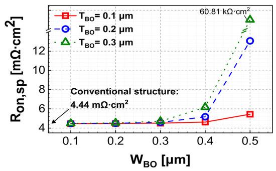
Figure 2. Ron,sp of the 1.2 kV SiC MOSFETs with the conventional structure and devices with buried oxides according to the WBO and TBO (VGS = 18 V).
The 1.2 kV SiC MOSFETs with the buried oxides have higher Ron,sp than the device with the conventional structure. The Ron,sp of the devices with buried oxides increases sharply with the increasing TBO when the WBO is 0.4 μm or higher. To analyze the sharp increase in the Ron,sp of the devices with buried oxides when the WBO is 0.4 μm or greater, the total current density of the devices with buried oxides was analyzed.
Figure 3 illustrates the total current density of 1.2 kV SiC MOSFETs with the buried oxides. The total current density was derived when the devices with the buried oxides had VDS and VGS of 10 and 18 V, respectively. The buried oxide approaches the p-base region as the WBO increases from 0.3 to 0.5 μm, leading to a reduction in the current density flow through the JFET region. For the devices with the TBO of 0.3 μm, it is evident that the buried oxide significantly impedes current flow through the JFET region. This obstruction of the current flow in the JFET region results in an increase in accumulation resistance [19,20,21]. In the case of the device with the buried oxide, where the WBO is 0.5 and TBO is 0.3 μm, the Ron,sp of the device is 60.81 kΩ·cm2 because the current is rarely flowing through the JFET region. These results indicate that the WBO needs to be 0.4 μm or less to reduce the Ron,sp.
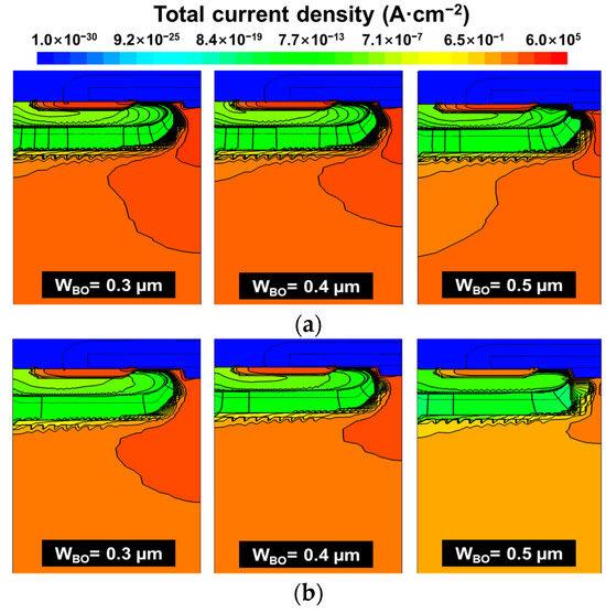
Figure 3. Total current density of the 1.2 kV SiC MOSFETs with the buried oxides (VDS= 10 and VGS= 18 V). The devices with the buried oxide with (a) a TBO of 0.2 μm and a WBO from 0.3 to 0.5 μm and (b) a TBO of 0.3 μm and a WBO from 0.3 to 0.5 μm.
The QGD of the 1.2 kV SiC MOSFET with the conventional structure and devices with the buried oxides according to the WBO and TBO are shown in Figure 4.
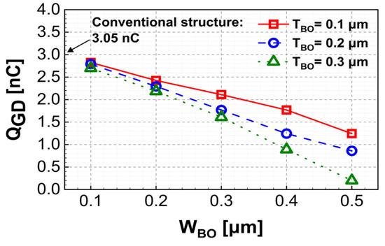
Figure 4. QGD of the 1.2 kV SiC MOSFETs with the conventional structure and devices with the buried oxides according to the WBO and TBO.
The QGD was determined by calculating the shift in gate charge between the two points where the slope of the Vgs−QG curve exhibits the maximum value [13,14]. In contrast to Figure 2, the QGD of the devices with the buried oxides is lower than that of the device with the conventional structure. This tendency becomes more noticeable as the WBO and TBO increase. When the devices have buried oxides with larger WBO and TBO, the area where the gate and the drain overlap is reduced, leading to a decrease in CGD between the gate and the drain [5,13,14].
Figure 5 shows the Eox,max of the 1.2 kV SiC MOSFET with the conventional structure and devices with the buried oxides according to the WBO and TBO. The Eox,max of the devices with the buried oxides is lower than that of the device with the conventional structure because the buried oxide is effective in dispersing the electric field at the gate oxide [13,14]. The Eox,max of the devices with buried oxide decreases as the WBO increases from 0.1 to 0.3 μm. However, the Eox,max of the devices with buried oxide increases as the WBO increases from 0.4 to 0.5 μm. The electric field distribution of 1.2 kV SiC MOSFETs with buried oxides according to the WBO and TBO was analyzed to figure out the cause of the increase in the Eox,max of the devices with the buried oxides when the WBO is 0.4 μm or greater.
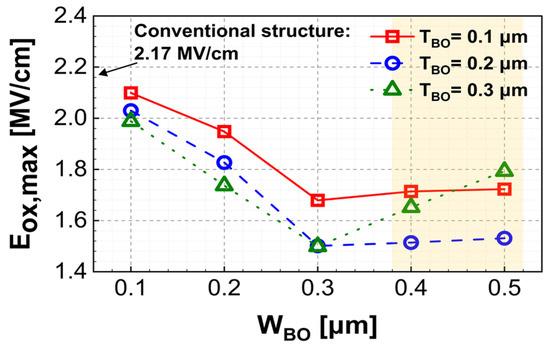
Figure 5. Eox,max of the 1.2 kV SiC MOSFETs with the conventional structure and devices with the buried oxides according to the WBO and TBO.
Figure 6a,b are the electric field distribution of the devices with the TBO of 0.4 and 0.5 μm, respectively. The respective Eox,max and locations where the electric field concentrates at the buried oxide are noted within each figure. The p-base has the highest Al concentration at a distance of 0.4 μm from the surface of the N-drift layer. At this point, the width of the JFET is 0.5 μm based on the half-cell. Therefore, the devices with the buried oxides and with a TBO of 0.3 μm are positioned closer to the junction between the p-base and the JFET than those with a TBO of 0.1 and 0.2 μm. Since the electric field is concentrated at the junction between the p-type and n-type semiconductors, the devices with the buried oxides with a TBO of 0.3 μm have high Eox,max due to the influence of the concentrated electric field at the junction between the p-base and the JFET [5,19,22,23]. When the WBO is 0.3 μm or less, the buried oxide is far enough away from the junction between the p-base and the JFET to prevent this phenomenon. However, when the WBO is 0.4 μm or greater, the buried oxide approaches the junction between the p-base and the JFET, causing an increase in Eox,max. This increase in Eox,max is particularly pronounced when the TBO is 0.3 μm.
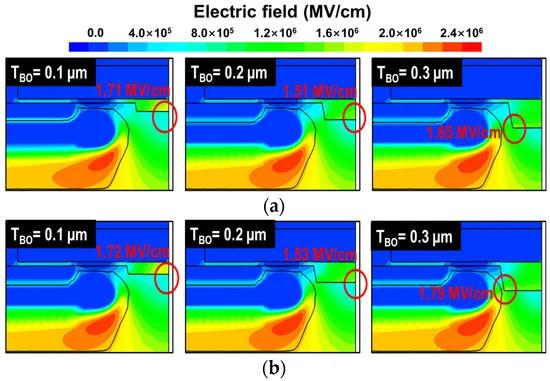
Figure 6. Electric field distribution of the 1.2 kV SiC MOSFETs with the buried oxides in the off state (VDS = 1200 V) with (a) a WBO of 0.4 and (b) a WBO of 0.5 µm.
The devices with buried oxides, where the WBO is greater than 0.4 μm, exhibit a significant increase in Ron,sp compared to the other devices with the buried oxides. Among the devices with the buried oxides where the WBO is 0.3 μm or less, the device with the buried oxide with a WBO of 0.3 and a TBO of 0.3 μm has the smallest QGD and Eox,max. Therefore, the optimal conditions for the WBO and TBO were chosen as 0.3 and 0.3 µm, respectively.
We compared the switching characteristics of the device with the conventional structure and the device with the buried oxide under optimal conditions (WBO = 0.3 and TBO = 0.3 μm). The used circuit for switching characteristics is shown in Figure 7. The circuit of Figure 7 was designed based on the settings of the Keysight PD1550A Double Pulse Analyzer. The gate voltage for switching the devices was switched from −5 to 18 V and the drain supply voltage was set to 800 V. Resistance of the gate and the load of the inductor were set to 10 Ω and 120 µH, respectively. The Etotal was calculated as the integral of the product of Id and Vds during the time which the device was switched [24].
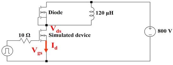
Figure 7. Circuit for switching simulations to compare the Etotal of the device with the conventional structure and the device with the buried oxide under optimal conditions (WBO = 0.3 and TBO = 0.3 µm).
Figure 8 and Figure 9 are the turn-on and turn-off switching characteristics of the 1.2 kV SiC MOSFETs with the conventional structure and the device with the buried oxide under optimal conditions (WBO = 0.3 and TBO = 0.3 µm), respectively. The Vgs, Vds and Id of the device with the buried oxide (WBO = 0.3 and TBO = 0.3 µm) vary more sharply during the switching process than the device with the conventional structure. Because the device with the buried oxide (WBO = 0.3 and TBO = 0.3 µm) has lower QGD than the device with the conventional structure, the device with the buried oxide (WBO = 0.3 and TBO = 0.3 µm) has fast rates of charge and discharge [5,6,7]. The device with the buried oxide (WBO = 0.3 and TBO = 0.3 µm) has lower power dissipated during the switching process than the device with the conventional structure.
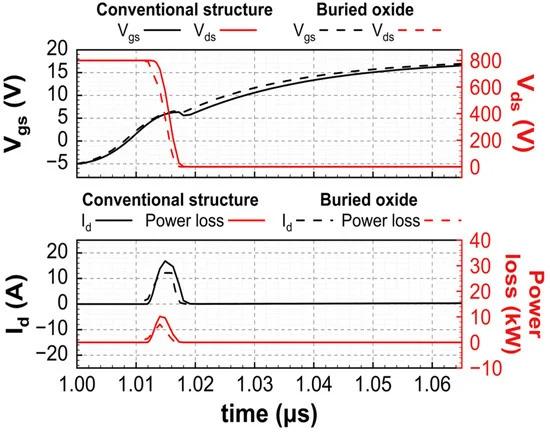
Figure 8. The turn-on switching characteristics of the 1.2 kV SiC MOSFETs with the conventional structure and the device with the buried oxide under optimal conditions (WBO = 0.3 and TBO = 0.3 µm).
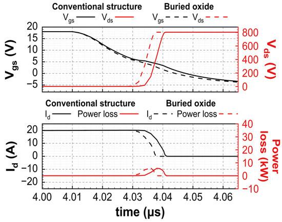
Figure 9. The turn-off switching characteristics of the 1.2 kV SiC MOSFETs with the conventional structure and device with the buried oxide under optimal conditions (WBO = 0.3 and TBO = 0.3 µm).
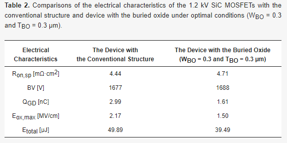
The electrical characteristics of the 1.2 kV SiC MOSFETs with the conventional structure and the device with the buried oxide (WBO = 0.3 and TBO = 0.3 µm) are summarized in Table 2. The Ron,sp, QGD and Eox,max of the device with the buried oxide (WBO = 0.3 and TBO = 0.3 μm) are 4.71 mΩ·cm2, 1.61 nC and 1.50 MV/cm, respectively. The device with the buried oxide (WBO = 0.3 and TBO = 0.3 μm) showed a 46.11% decrease in QGD, a 30.88% decrease in Eox,max and only a 6.10% increase in Ron,sp compared to the device with the conventional structure. In addition, the Etotal of the 1.2 kV SiC MOSFET with the buried oxide (WBO = 0.3 and TBO = 0.3 μm) is lower than the device with the conventional structure. The Etotal of the device with the buried oxide (WBO = 0.3 and TBO = 0.3 μm) is 39.49 µJ, which is 20.84% lower than that of the device with the conventional structure. These results demonstrate that buried oxide can improve the switching characteristics of 1.2 kV SiC MOSFETs.
Table 2. Comparisons of the electrical characteristics of the 1.2 kV SiC MOSFETs with the conventional structure and device with the buried oxide under optimal conditions (WBO = 0.3 and TBO = 0.3 µm).
4. Conclusions
The 1.2 kV SiC MOSFET with the buried oxide was introduced to improve the switching characteristics of the device by reducing the QGD. By analyzing the Ron,sp, QGD and Eox,max of the devices with the buried oxides according to the WBO and TBO, it was shown that the device with the buried oxide has the best performance when the WBO and TBO are 0.3 and 0.3 µm, respectively. The Eox,max and Etotal of the device with the buried oxide (WBO = 0.3 and TBO = 0.3 µm) were 1.50 MV/cm and 39.49 µJ, resulting in 30.88% and 20.84% reductions compared to those with the conventional structure. The Ron,sp of the device with the buried oxide (WBO = 0.3 and TBO = 0.3 µm) increased by only 6.10% compared to that of the device with the conventional structure.