Abstract
In this paper, we propose an optimized device structure with a highly stable process that addresses threshold voltage shift issues in the String-Select-Line (SSL) and Ground-Select-Line (GSL) gates using ferroelectric memory in 3D NAND flash memory applications. The proposed device utilizes nickel (Ni) instead of tungsten (W) for the GSL and SSL gates, enabling optimized polarization properties during the annealing process and leveraging the disparity in thermal expansion coefficients. Notably, the difference in thermal expansion coefficient from tungsten (W), employed in other Word Line (WL) gates, allows effective control over polarization properties. To validate the proposed structure, we fabricated and measured a Metal–Ferroelectric–Insulator–Silicon (MFIS) capacitor utilizing Hafnium–Zirconium Oxide (HZO) material. The measurement results indicate that a change in the upper metal layer results in a more than fivefold increase in the variance of polarization characteristics between the WL gates (responsible for the memory function) and the SSL and GSL gates dedicated to channel control. In addition, process simulation was conducted using the same device structure, confirming the application of tensile stress to the HZO thin film in the case of a W electrode and compressive stress in the case of a Ni electrode. Furthermore, applying this controlled polarization characteristic parameter to the 3D NAND flash memory structure revealed a reduction in the threshold voltage shift of the control gate from a previous change of 2.6 V or more to 0.05 V, facilitating stable control.
Keywords: 3D NAND; charge trap flash (CTF); ferroelectric; stress
1. Introduction
Since the initial introduction of the 3D NAND flash memory device structure reported in 2007 [1], many memory companies have concentrated on integration and performance enhancement using this structure. They have announced diverse research outcomes and product releases, contributing to the growth of the memory market and gradually replacing the conventional hard disk market [2,3]. Furthermore, a significant advantage of the vertical stacking structure, inherent in 3D NAND flash memory, is no need for a lithography process, resulting in a substantial reduction in manufacturing costs as the number of stack layers increases. Currently, the number of stack layers has surpassed 256, with a further increase to a range of 300 to 500 layers projected in the near future [4].
Nevertheless, recent research outcomes show that the 3D NAND flash memory structure is vulnerable to various issues, including electrical issues such as threshold voltage instability and operational current fluctuations induced by temperature variations, as well as mechanical issues such as silicon substrate bending caused by differences in stress characteristics between different materials. Although advancements in process technology have alleviated these issues, it is anticipated that such efforts will encounter various limits.
During the initial phases of 3D NAND flash memory development, a notable departure from conventional 2D NAND flash memory technology was the adoption of Charge Trap Flash (CTF) memory as the memory architecture. CTF memory employs silicon nitride, a material characterized by significantly restricted electron mobility, as the electron storage layer. In contrast to traditional flash memory utilizing polysilicon for the electronic storage layer, the use of CTF memory has resulted in substantial enhancements in stability and reliability [5]. These inherent advantages have played a pivotal role in expediting the rapid progression of 3D NAND flash memory technology. This simple yet efficient CTF memory has been developed since the inception of 3D NAND flash memory and has recently achieved technological advances to the extent that it can operate up to 16 levels of Quad-Level Cells (QLCs) [6]. However, this structure has suffered from various problems, the most significant of which is power consumption due to very slow operating speed and high operating voltage [7].
To address this issue, research on next-generation memory to replace CTF memory in current 3D NAND flash memory structures has been conducted [8]. Ferroelectric memory, among these new concepts, offers advantages similar to resistance change memory, such as low power consumption and high operating speed. Its structure closely resembles the oxide–nitride–oxide (ONO) structure used in CTF flash memory [9,10,11,12]. Consequently, the NAND flash memory structure utilizing ferroelectric memory retains the fundamental advantage of seamlessly preserving the existing NAND flash memory structure and operational methodology. Owing to these inherent strengths, research on applying ferroelectric memory to the 3D NAND structure has progressed rapidly compared to other memory devices, with some instances of tangible devices being fabricated to demonstrate the feasibility of the aforementioned approach [13].
However, there are still numerous challenges that must be addressed before ferroelectric memory can be fully integrated into 3D NAND flash memory. Among these challenges, this paper specifically addresses the issues associated with String Select Line (SSL) and Ground Select Line (GSL), responsible for the individual control of each channel string. As elaborated in the next section, the SSL and GSL within the 3D NAND flash memory structure play a crucial role in managing the current flow across hundreds of thousands of channel strings. Specifically, to address the low current mobility of the polysilicon channel, it is crucial for the SSL and GSL gates to control channels, ensuring stable operation in the off state while facilitating optimal current flow in the on state.
Additionally, to streamline the process, the current 3D NAND flash memory structure fundamentally adopts the same memory storage structure in the gate insulation films of the SSL and GSL, similar to other Word Lines (WLs). This approach did not pose significant challenges, given the minimum operating voltage of 10 V or higher associated with CTF memory. However, it raises substantial concerns at low operating voltages of 2 to 4 V, which are relevant to ferroelectric memory. In essence, the operating voltages of SSL and GSL at 4 to 5 V, which presented no issues in the 3D NAND flash memory structure employing CTF memory, can perturb the threshold voltage of the two control gates when ferroelectric memory is implemented. Nevertheless, addressing this issue by separately forming a gate-insulating film for the SSL and GSL can result in a highly intricate process and increased costs within the 3D NAND flash memory structure.
Therefore, to fundamentally address this issue, a novel method is required to eliminate the memory characteristics of ferroelectric memory, which is used as a gate-insulating film between the SSL and GSL. This should be achieved while preserving the current 3D NAND flash memory process to the greatest extent possible. Fortunately, one of the unique features of ferroelectric memory is its ability to modulate memory characteristics in response to changes in mechanical stress, such as tensile or compressive stress. Focusing on these characteristics, this paper presents an optimized device structure with a stable process and operational outcomes that employ gate metals of the SSL, GSL, and other WLs as different materials. This approach leverages stress changes to eliminate the memory characteristics of the SSL and GSL in the same process while retaining the memory characteristics of WLs, ensuring a stable threshold voltage.
2. Details of the Proposed Structures and Process
Figure 1a and Figure 1b, respectively, show the conventional and proposed ferroelectric memory-based 3D NAND flash memory structures. In the latter, the electrodes of the SSL and GSL gates are replaced with nickel (Ni) from tungsten (W) used in the former. As shown in Figure 1a, the conventional structure is configured with the SSL and GSL gate-insulating films, which are formed of Hafnium–Zirconium Oxide (HZO) with the same ferroelectric memory function as other WLs. This structure is employed to reduce manufacturing costs associated with the 3D NAND flash memory, achieving the creation of the string hole, channel layer, and macaroni oxide (M-oxide) layer with a minimized number of process steps. However, the currently used CTF in 3D NAND flash memory has a minimum operating voltage of 10V, causing the threshold voltages of the SSL and GSL gates to remain unchanged with turn-on voltages of approximately 4 V to 5 V. This issue arises when ferroelectric memory is applied. In the red elliptical region of Figure 1a, the threshold voltage of HZO can easily fluctuate whenever a turn-on voltage is applied due to the low operating voltage specific to ferroelectric memory. This may lead to a malfunction of the ferroelectric memory as a control gate because the threshold voltage shifts in the negative direction when a positive voltage is applied.

Figure 1. (a) Conventional one-string structure of a ferroelectric memory-based 3D NAND flash memory and (b) proposed structure.
To address this issue, the proposed structure replaces the material of the gate electrodes for SSL and GSL from W to Ni, as illustrated in Figure 1b. The electrode employed in the WL gate utilizes a metal to enhance the polarization properties of the ferroelectric memory through mechanical stress during the ferroelectric thermal process. Simultaneously, a metal with contrasting properties is employed for the SSL and GSL gates [14]. After the thermal process, the ferroelectric materials of the SSL and GSL simply exhibit insulative or anti-ferroelectric characteristics, suppressing the ferroelectric properties. In this way, the threshold voltages of the SSL and GSL gates can always be maintained at a constant level.
Figure 2 illustrates the fabrication process of the proposed structure. Figure 2a shows the GSL electrode formation process. During the formation process, the silicon oxide and nickel metal electrode are deposited and immediately etched. Subsequently, the etched hole is filled with a dummy material that is easy to etch in the subsequent process. Figure 2b shows the initial stage of the gate replacement process [2] for the electrode formation of the WL. Here, silicon nitride (Si3N4) layers and insulating silicon oxide (SiO2) layers are alternately deposited. Subsequently, the deposited layer is etched simultaneously, and the resulting hole is filled with the same dummy material employed in the process shown in Figure 2a. In Figure 2c, nickel is utilized as the SSL gate electrode material, and the identical structure is formed as in the GSL formation. Similar to the formation of the GSL electrode described earlier, the key aspect of this process is the direct deposition followed by metal etching. This is feasible because, unlike WLs, which demand etching for a minimum of 200 metal layers, the gate replacement process is unnecessary as only one metal layer is etched. Figure 2d shows an extension of the double-stacking process [15] currently employed in the 3D NAND flash process, where the dummy material is removed, and the ferroelectric material HZO, polysilicon channel, and M-oxide layers are sequentially deposited. Figure 2e shows the process where the Si3N4 layer is removed using an etchant that reacts only to Si3N4. In Figure 2f, a W electrode is deposited in the vacancy to complete the gate substitution process. Finally, in Figure 2g, the ferroelectric properties of HZO are activated through an annealing process between approximately 600 and 700 °C. In this process, the polarization properties of the ferroelectric layers of the SSL and GSL are suppressed by metals with different coefficients of thermal expansion. Conversely, the ferroelectric layer of the WL has its polarization properties activated, enabling memory operation. More importantly, these insulating film layers with different functions can be created simultaneously through a single annealing process. This approach is highly efficient in a 3D NAND flash memory structure, where adding a new process is challenging due to cost or process complexity.

Figure 2. Formation process of the upper BL contact in the proposed structure. (a): GSL formation process, (b–f): “Gate Replacement” process for WLs formation. And ferroelectric materials, channels, M-oxide deposition process, (f): SSL formation process, (g): GSL through annealing process, ferroelectric material optimization process of SSL gate.
3. Simulation Results and Discussion
3.1. Simulated Structures, Models, and Parameters
Figure 3 shows the detailed device structure employed in the simulation, configured as a virtual gate-all-around (GAA) structure [16]. The implemented structure, which is represented by only half of the structure depicted in Figure 3a, was used to evaluate the operation of the fully vertical channel 3D NAND string. In addition, each contact was composed as follows. First, the Common-Source-Line (CSL) contact serves as the source for the entire channel, while the GSL located on it controls the contact between the CSL and the channel. Second, the 10 WLs present on it function as gates. Additionally, the SSL contact controls the contact between the Bit Line (BL) and the channel at the top, and the upper BL acts as the drain.

Figure 3. Detailed device structure with doping profile. (a) Schematic of the 10 stacked memory cells, Word Lines WL0 to WL9, and select transistors GSL, SSL, BL, and CSL; and (b) enlarged view of the device structure.
Figure 3b shows an enlarged view of the device structure employed in the simulation, including the dimensions. First, the polysilicon channel had a thickness of 10 nm, followed by the HZO layer with a thickness of 10 nm for the memory function. The thickness of W, which is a WL metal, was set to 30 nm. The lengths of the SSL and GSL gates were set to 100 nm, suppressing leakage current flowing to the BL and CSL, and enhancing gate control capability. Finally, the doping concentration of the CSL, which was the polysilicon contact, was set to 1020 cm−3.
Finally, various parameters (mobility, trap distribution, etc.) and physical models used in the polysilicon channel and contact were verified using models reported in [16].
3.2. Simulation Analysis on Problems Arising from 3D NAND Flash Structure Based on Conventional Ferroelectric Memory
In the simulation for the conventional ferroelectric memory, the saturation polarization (Ps) was set to 60 μC/cm2, the remanent polarization (Pr) was set to 45 μC/cm2, and the coercive field (Ec) was set to 4 MV/cm for the ferroelectric material. Here, the polarization characteristic parameter used in this work represents one of the largest values of ferroelectric polarization characteristics to date [17]. Thus, these ferroelectric parameters can be applied to the current 3D NAND flash structures with conventional ferroelectric memory, especially based on the significantly high Ec at which the polarization characteristics begin to change [17].
Figure 4a,b show the I–V results of the GSL and SSL gates, respectively. These respective graphs depict the HZO states after applying the turn-on voltage (4 V) during the operation of reading the memory state of the WL, which is different from the initial state. This indicates that the I–V curves of the GSL and SSL gates have significantly shifted to the negative region after applying the turn-on voltage, more distinctly for the GSL than the SSL. This observation is attributed to the difference in the size of the applied electric field, depending on whether the adjacent electrode is a CSL (0 V) or BL (1 V). However, the threshold voltage has shifted to the negative direction by approximately 2 V in both gates, indicating that normal channel control cannot be attained in the current 3D NAND flash structures with conventional ferroelectric memory. Furthermore, despite the utilization of a highly favorable polarization parameter, more concern arises from the instability of the threshold voltage. Particularly, even the commonly employed turn-on voltage of 4 V in current 3D NAND flash memory cannot be applied effectively, even at an Ec of 4 MV/cm. Overcoming this challenge involves enhancing resistance to the applied electric field by either further increasing Ec or thickening the ferroelectric layer. However, such approaches result in an elevated voltage requirement for memory operations, potentially compromising the low power consumption advantage inherent to ferroelectric memory. Hence, the most effective approach to address this issue entails stabilizing the threshold voltage within the GSL and SSL gates through modulation of the polarization characteristics inherent in the ferroelectric layer, which will be described in the next section.

Figure 4. I–V results of (a) GSL gate and (b) SSL gate.
3.3. Analysis Results from Actual Device Measurement and Process Simulation
As previously described, a specific process to ensure stable control of the GSL and SSL gates needs to be involved in giving non-ferroelectric properties to the insulating film of the GSL and SSL gates, while simultaneously providing ferroelectric properties to the insulating film of WL gates. Thus, in this section, the device fabrication and measurement are presented to validate the proposed ideas, while analyzing the results of process simulations for a more in-depth understanding.
Figure 5 shows the device fabrication process designed to verify the change in ferroelectric properties according to the change in the upper electrode. Initially, a Si (100) substrate was subjected to atomic layer deposition (ALD) for the deposition of 2 nm HfO2 thin films. Subsequently, HZO thin films with thicknesses of 4.5, 9, 13.5, 18, and 22.5 nm were deposited using ALD at a chamber temperature of 280 °C. Following this, a 100 nm thickness of W and Ni was deposited via DC sputtering, utilizing a 300 μm diameter shadow mask. The deposited Metal–Ferroelectric–Insulator–Semiconductor (MFIS) capacitor underwent a 10 s annealing process at 600 °C in a N2 atmosphere using a Rapid Thermal Annealing (RTA) system to induce crystallization in the HZO thin film [11]. Concurrently, the stress characteristics imposed on the HZO thin film during the annealing process are analyzed through process simulation.

Figure 5. Actual device fabrication and its process.
Figure 6a,b show the polarization characteristics of the manufactured device according to the electric field when the top electrode material used is W and Ni, achieving 2Pr of 14.9 μC/cm2 and 2.9 μC/cm2, respectively. This difference is attributed to stress variations caused by the varying coefficients of thermal expansion of the upper electrode, similar to the tendency found in prior research [14].
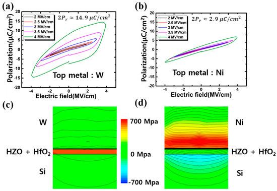
Figure 6. Measured polarization characteristics of the fabricated device according to electric field when the top electrode material is (a) W and (b) Ni, and stress variations in the annealing process through process simulation when the top electrode material is (c) W and (d) Ni.
Figure 6c,d show the stress variations through process simulation, revealing a substantial tensile stress (depicted in red in Figure 6c) applied to the HZO layer when W is used, and a significant compressive stress (depicted in green in Figure 6d) when Ni is used, respectively.
Based on the above device measurements and process simulations, effective control for the polarization properties of the adjacent ferroelectric can be achieved by selecting W with a low coefficient of thermal expansion as the WL gate material, while selecting Ni with a high coefficient of thermal expansion as the SSL and GSL gate materials. Furthermore, this approach allows the enhanced stability of the gate by effectively suppressing the polarization properties of the SSL and GSL gates.
Subsequently, the variation in stress with thickness, specifically the impact of HZO thin film thickness on polarization characteristics, was investigated. In general, an in-crease in the thickness of ferroelectric materials leads to a corresponding increase in polarization properties. However, there is a limit to this improvement, and concurrently, as the polarization properties of the SSL and GSL gates increase, the stability of these gates may decrease. Therefore, it is crucial to determine the optimal thickness at which the difference in polarization properties between the WL gates responsible for memory operation and the SSL and GSL gates responsible for channel control can be maximized, enhancing reliability and stability in the GSL and SSL gates.
The stress applied to the ferroelectric material confirmed in Figure 7a continued to increase with the thin film thickness. However, the polarization characteristics confirmed in Figure 7b tended to increase until the HZO thin film thickness reached 18 nm and then decreased. These results represent that the development of the Orthorhombic (O)-phase, indicative of the ferroelectric polarization, is proportional to some extent to the increase in thickness, but decreases beyond a specific threshold [18]. In summary, the difference in the polarization characteristics of W and Ni were the largest at the point where the thickness of the HZO thin film reached 9.5 nm. When exceeding this threshold, the polarization characteristics of the Ni electrode rapidly increased, leading to the instability of the threshold voltages of the SSL and GSL gates. Therefore, in this paper, the optimal thickness for controlling ferroelectric properties through stress change caused by the annealing process was set to 9.5 nm.
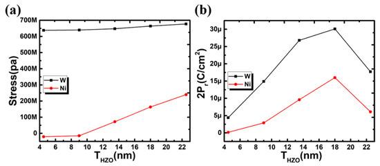
Figure 7. Stress and polarization characteristics according to the thickness of the HZO thin film. (a) is the result of stress and (b) is the polarization result.
3.4. Simulation Verification in Proposed 3D NAND Flash Structure
The operational characteristics of the SSL and GSL gates were verified and analyzed through simulation by changing the electrodes of the SSL and GSL using the same structure used in the previous simulation described in Section 3.2. The applied parameters are listed in Table 1.

These parameters were derived from the previous actual device measurement results conducted at an HZO thin film thickness of 9.5 nm. This parameter selection was based on the previous observation that the difference in polarization properties was most distinctive, while inhibiting the polarization properties of Ni at this thickness was most effective.
By applying the polarization parameters derived from the previous device measurement, a memory window of 2.64 V was obtained in WL4, as shown in Figure 8a. Conversely, Figure 8b,c reveal that the threshold voltage variations in GSL and SSL are only 0.04 V and 0.01 V, respectively, which are minimal. Therefore, this demonstrates that the threshold voltages of GSL and SSL can be controlled very stably in the 3D NAND flash memory structure using the proposed process.
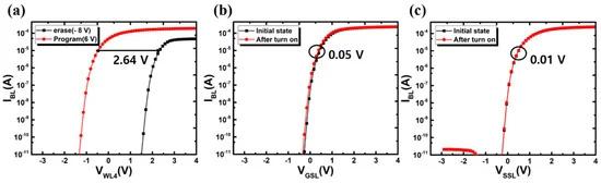
Figure 8. Memory operation results in (a) WL4, (b) GSL, and (c) SSL.
4. Conclusions
In this paper, an innovative approach was devised to address the challenge of uncontrolled threshold voltages in GSL and SSL gates within a 3D NAND flash memory structure employing ferroelectric memory. The issue arises due to the shared ferroelectric layer among all gates. To mitigate this, the metal composition of the SSL and GSL gates was changed to Ni, a metal exhibiting a different coefficient of thermal expansion from the gate metal (W) used in WLs. The novel structure and process were presented to suppress the polarization properties of the ferroelectric insulating films in GSL and SSL gates through an annealing process.
The proposed approach was subjected to extensive examination through actual device measurements, process simulations, and device simulations. The device measurements revealed that the divergence in stress, resulting from the different coefficients of thermal expansion between W and Ni, induced more than a fivefold difference in polarization characteristics. This stress difference was substantiated through process simulations properly reproducing the operational procedures.
Upon implementing the secured polarization characteristics in the 3D NAND flash memory structure, it was observed that the threshold voltage change in GSL and SSL gates was only 0.05 V, even when the memory window of WLs gates was set at 2.64 V. These results demonstrate the successful enhancement of reliability and stability in GSL and SSL gates when incorporating ferroelectric memory into the prospective 3D NAND flash memory structures.
Based on these results, we will first manufacture 2D FeFETs in subsequent studies, and measure and verify whether the operation of GSL and SSL transistors can be as stable as the simulation results. Then, 3D GAA structures will be manufactured to verify operational performance.